- 您現(xiàn)在的位置:買賣IC網(wǎng) > PDF目錄98299 > TS8388BMFS9NC3 (E2V TECHNOLOGIES PLC) 1-CH 8-BIT PROPRIETARY METHOD ADC, PARALLEL ACCESS, CQFP68 PDF資料下載
參數(shù)資料
| 型號: | TS8388BMFS9NC3 |
| 廠商: | E2V TECHNOLOGIES PLC |
| 元件分類: | ADC |
| 英文描述: | 1-CH 8-BIT PROPRIETARY METHOD ADC, PARALLEL ACCESS, CQFP68 |
| 封裝: | CERAMIC, QFP-68 |
| 文件頁數(shù): | 27/62頁 |
| 文件大小: | 1267K |
| 代理商: | TS8388BMFS9NC3 |
第1頁第2頁第3頁第4頁第5頁第6頁第7頁第8頁第9頁第10頁第11頁第12頁第13頁第14頁第15頁第16頁第17頁第18頁第19頁第20頁第21頁第22頁第23頁第24頁第25頁第26頁當前第27頁第28頁第29頁第30頁第31頁第32頁第33頁第34頁第35頁第36頁第37頁第38頁第39頁第40頁第41頁第42頁第43頁第44頁第45頁第46頁第47頁第48頁第49頁第50頁第51頁第52頁第53頁第54頁第55頁第56頁第57頁第58頁第59頁第60頁第61頁第62頁
33
0860E–BDC–05/07
e2v semiconductors SAS 2007
TS8388B
8.4.3
Single-ended ECL Clock Input
In single-ended configuration enter on CLK (resp. CLKB) pin, with the inverted phase clock input pin
CLKB (respectively CLK) connected to –1.3V through the 50
termination resistor.
The inphase input amplitude is 1V peak to peak, centered on –1.3V common mode.
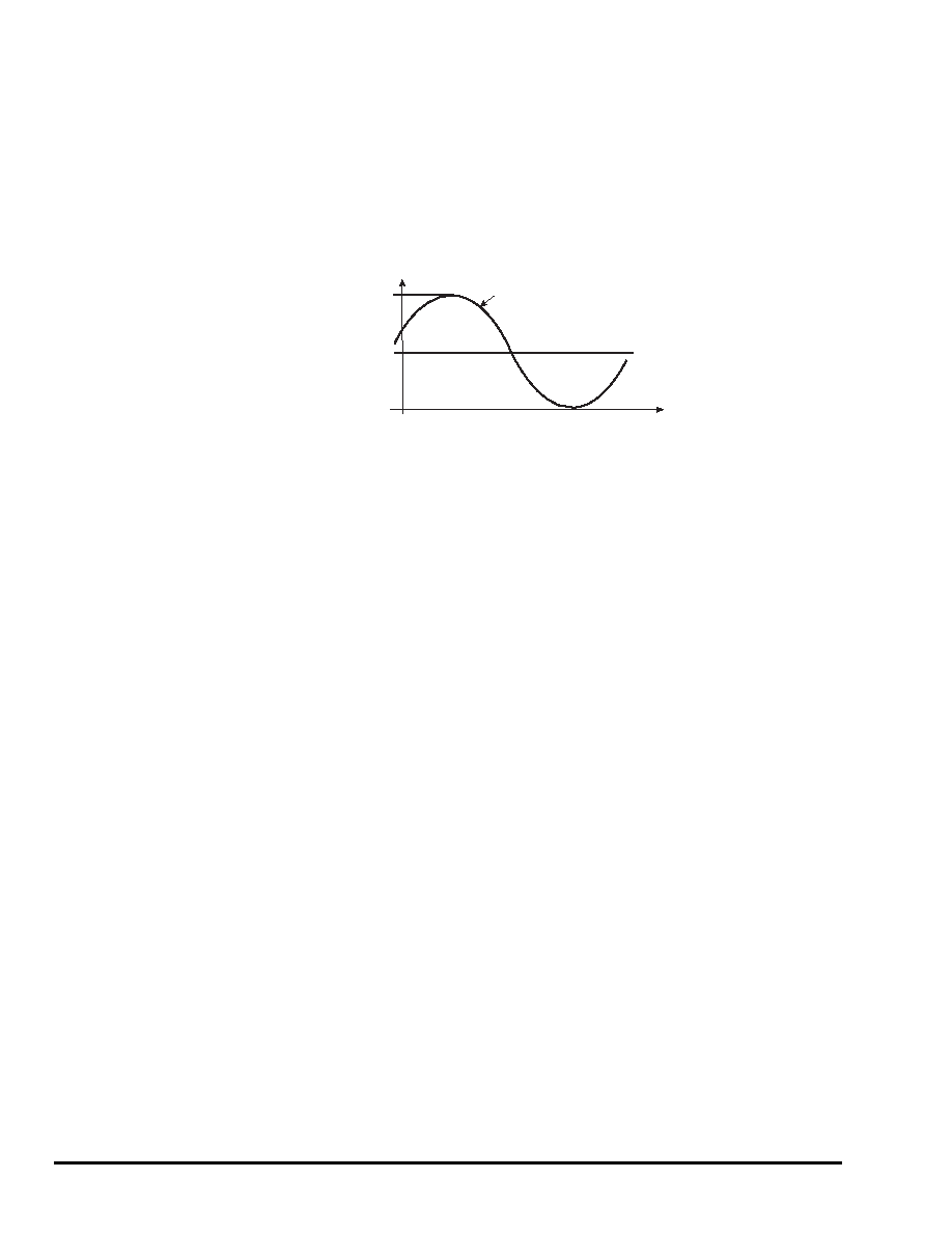
Figure 8-5.
Single-ended Clock Input (ECL):
VCLK Common Mode = –1.3V; VCLKB = –1.3V
8.5
Noise Immunity Information
Circuit noise immunity performance begins at design level.
Efforts have been made on the design in order to make the device as insensitive as possible to chip
environment perturbations resulting from the circuit itself or induced by external circuitry (Cascode
stages isolation, internal damping resistors, clamps, internal (on-chip) decoupling capacitors).
Furthermore, the fully differential operation from analog input up to the digital outputs provides enhanced
noise immunity by common mode noise rejection.
Common mode noise voltage induced on the differential analog and clock inputs will be canceled out by
these balanced differential amplifiers.
Moreover, proper active signals shielding has been provided on the chip to reduce the amount of cou-
pled noise on the active inputs.
The analog inputs and clock inputs of the TS8388B device have been surrounded by ground pins, which
must be directly connected to the external ground plane.
8.6
Digital Outputs
The TS8388B differential output buffers are internally 75
loaded. The 75 resistors are connected to
the digital ground pins through a –0.8V level shift diode (see Figure 8-6, Figure 8-7, Figure 8-8 on page
36).
The TS8388B output buffers are designed for driving 75
(default) or 50 properly terminated imped-
ance lines or coaxial cables. An 11 mA bias current flowing alternately into one of the 75
resistors
when switching ensures a 0.825V voltage drop across the resistor (unterminated outputs).
The V
PLUSD positive supply voltage allows the adjustment of the output common mode level from –1.2V
(V
PLUSD = 0V for ECL output compatibility) to +1.2V (VPLUSD = 2.4V for LVDS output compatibility).
Therefore, the single-ended output voltages vary approximately between –0.8V and –1.625V, (outputs
unterminated), around –1.2V common mode voltage.
Three possible line driving and back-termination scenarios are proposed (assuming V
PLUSD = 0V):
-1.8V
-0.8V
t
[V]
VCLK
VCLKB = -1.3V
相關PDF資料 |
PDF描述 |
|---|---|
| TS8388BCGL | 1-CH 8-BIT PROPRIETARY METHOD ADC, PARALLEL ACCESS, CBGA68 |
| TS8388BMFS | 1-CH 8-BIT PROPRIETARY METHOD ADC, PARALLEL ACCESS, CQFP68 |
| TS8388BVGL | 1-CH 8-BIT PROPRIETARY METHOD ADC, PARALLEL ACCESS, CBGA68 |
| TS8388BMFSB/T | 1-CH 8-BIT PROPRIETARY METHOD ADC, PARALLEL ACCESS, CQFP68 |
| TS8388BVFS | 1-CH 8-BIT PROPRIETARY METHOD ADC, PARALLEL ACCESS, CQFP68 |
相關代理商/技術參數(shù) |
參數(shù)描述 |
|---|---|
| TS8388BMFSB/Q | 制造商:e2v technologies 功能描述:ADC 8-BIT 1 GSPS - Trays |
| TS8388BVF | 制造商:e2v technologies 功能描述:ADC 8-BIT 1 GSPS - Trays |
| TS8388BVFS | 制造商:e2v technologies 功能描述:ADC 8-BIT 1 GSPS - Trays |
| TS8388BVGL | 制造商:e2v technologies 功能描述:ADC 8-BIT 1 GSPS - Trays |
| TS8388BVGL (+LID) | 制造商:e2v technologies 功能描述:ADC 8-BIT 1 GSPS - Trays |
發(fā)布緊急采購,3分鐘左右您將得到回復。