- 您現(xiàn)在的位置:買賣IC網(wǎng) > PDF目錄98299 > TS8388BVFS9NC3ZB9 (E2V TECHNOLOGIES PLC) 1-CH 8-BIT PROPRIETARY METHOD ADC, PARALLEL ACCESS, CQFP68 PDF資料下載
參數(shù)資料
| 型號: | TS8388BVFS9NC3ZB9 |
| 廠商: | E2V TECHNOLOGIES PLC |
| 元件分類: | ADC |
| 英文描述: | 1-CH 8-BIT PROPRIETARY METHOD ADC, PARALLEL ACCESS, CQFP68 |
| 封裝: | CERAMIC, QFP-68 |
| 文件頁數(shù): | 25/43頁 |
| 文件大小: | 825K |
| 代理商: | TS8388BVFS9NC3ZB9 |
第1頁第2頁第3頁第4頁第5頁第6頁第7頁第8頁第9頁第10頁第11頁第12頁第13頁第14頁第15頁第16頁第17頁第18頁第19頁第20頁第21頁第22頁第23頁第24頁當前第25頁第26頁第27頁第28頁第29頁第30頁第31頁第32頁第33頁第34頁第35頁第36頁第37頁第38頁第39頁第40頁第41頁第42頁第43頁
TS8388BFS
31/42
Preliminary Beta Site
7.4.3.
SINGLE ENDED ECL CLOCK INPUT
In single–ended configuration enter on CLK ( resp. CLKB ) pin , with the inverted phase Clock input pin CLKB (respectively CLK) connected to -
1.3V through the 50 ohms termination resistor.
The inphase input amplitude is 1 Volt peak to peak, centered on -1.3 Volt common mode.
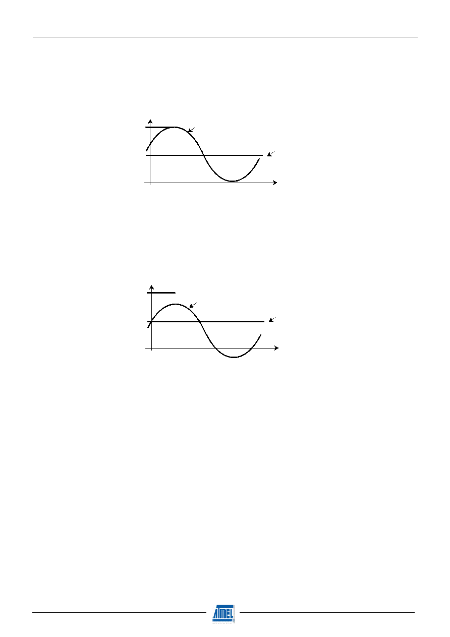
Single ended Clock input (ECL):
VCLK common mode = -1.3 Volt.
VCLKB = -1.3 Volt
-0.8V
[V]
t
-1.8V
VCLK
VCLKB = -1.3 V
7.5.
CLOCK SIGNAL DUTY CYCLE ADJUST
At fast sampling rates, ( 1 GSPS and above), the device performance ( especially the SNR ) may be improved by tuning the Clock duty cycle
(CLK,CLKB).
In single ended configuration, when using a sinewave clock generator, the clock signal duty cycle can be easily adjusted by simply offseting the
inphase clock signal using a biasing tee, (as the out of phase clock input is at ground level ).
Single ended Clock input (Inphase clock input common mode shifted)
VCLK common mode = -180mV
VCLKB = 0 Volt
[V]
t
VCLK - 180 mV
VCLKB = ( 0 V )
-0.5V
40 %
60 %
+0.5V
Note 1 : Do not exceed 10 dBm into the 50 ohms termination resistor for single clock input power level.
Note 2 : For an input CLK signal of 4 dBm into 50 ohms, the typical offset value to achieve a 40 / 60 clock duty cycle is -180 mV on CLK.
7.6.
NOISE IMMUNITY INFORMATIONS
Circuit noise immunity performance begins at design level.
Efforts have been made on the design in order to make the device as insensitive as possible to chip environment perturbations resulting from
the circuit itself or induced by external circuitry.
(Cascode stages isolation, internal damping resistors, clamps, internal (onchip) decoupling capacitors.)
Furthermore, the fully differential operation from analog input up to the digital outputs provides enhanced noise immunity by common mode
noise rejection.
Common mode noise voltage induced on the differential analog and clock inputs will be canceled out by these balanced differential amplifiers.
Moreover, proper active signals shielding has been provided on the chip to reduce the amount of coupled noise on the active inputs :
The analog inputs and clock inputs of the TS8388BFS device have been surrounded by ground pins, which must be directly connected to the
external ground plane.
相關PDF資料 |
PDF描述 |
|---|---|
| TS8388BVFS9QB3ZB9 | 1-CH 8-BIT PROPRIETARY METHOD ADC, PARALLEL ACCESS, CQFP68 |
| TS8388BMFS9QB1ZB9 | 1-CH 8-BIT PROPRIETARY METHOD ADC, PARALLEL ACCESS, CQFP68 |
| TS8388BCFS9NB2ZB9 | 1-CH 8-BIT PROPRIETARY METHOD ADC, PARALLEL ACCESS, CQFP68 |
| TS8388BVFS9QC1ZB9 | 1-CH 8-BIT PROPRIETARY METHOD ADC, PARALLEL ACCESS, CQFP68 |
| TS8388BCFS9QB1ZB9 | 1-CH 8-BIT PROPRIETARY METHOD ADC, PARALLEL ACCESS, CQFP68 |
相關代理商/技術參數(shù) |
參數(shù)描述 |
|---|---|
| TS8388BVGL | 制造商:e2v technologies 功能描述:ADC 8-BIT 1 GSPS - Trays |
| TS8388BVGL (+LID) | 制造商:e2v technologies 功能描述:ADC 8-BIT 1 GSPS - Trays |
| TS83C194 | 制造商:未知廠家 制造商全稱:未知廠家 功能描述:16-Bit Microcontroller |
| TS83C196KB-10 | 制造商:未知廠家 制造商全稱:未知廠家 功能描述:16-Bit Microcontroller |
| TS83C196KD | 制造商:未知廠家 制造商全稱:未知廠家 功能描述:Microcontroller |
發(fā)布緊急采購,3分鐘左右您將得到回復。