- 您現在的位置:買賣IC網 > PDF目錄382705 > U6057B Receiver for Point-to-Point Multiplex Systems PDF資料下載
參數資料
| 型號: | U6057B |
| 英文描述: | Receiver for Point-to-Point Multiplex Systems |
| 中文描述: | 接收機點至點多路傳輸系統 |
| 文件頁數: | 2/9頁 |
| 文件大小: | 89K |
| 代理商: | U6057B |
U6057B
TELEFUNKEN Semiconductors
Rev. A1, 03-Dec-97
Preliminary Information
2 (9)
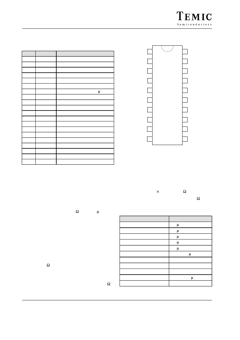
Pin Configuration
Table 1. Pin description
Pin
1
2
3
4
5
6
7
8
9
10
11
12
13
14
15
16
17
18
19
20
Symbol
GND
DIN
nc
P/S
CLK
nc
DOUT
nc
2/4
SYN
CO
PP
DT
nc
nc
nc
nc
OCS
V
stab
V
S
Function
Ground
Serial data input
Parallel/serial switch-over
Clock input for shift register
Serial data output for the C
2/4-fold comparison
Synchronization
Clock output for cascading
Program pin
Data input of data line
RC-oscillator input
Stabilized voltage
Supply voltage
1
2
3
4
5
6
7
8
10
9
19
18
17
16
14
15
13
12
11
20
P/S
CLK
13272
nc
DOUT
nc
2/4
DIN
nc
nc
nc
nc
nc
DT
PP
V
Stab
OSC
SYN
CO
GND
V
S
U6057B
Figure 2. Pinning of U6057B
Functional Description
Power Supply
For protection against interference and surges, the
U6057B must be equipped with an RC-circuit for current
limitation in the event of overvoltages and for buffering
in the event of voltage dips at V
S
.
Suggested dimensions: Rv = 510 , C
V
= 100 F
(see figure 3 )
An integrated 14-V Z-diode is located between V
S
and
GND.
Oscillator
All timing in the circuit is derived from an RC-oscillator.
The oscillator’s charging time t
1
is determined by an
external resistor, R
OSC
, and its discharge time t
2
by an
integrated 2-k resistor. Since the tolerance and
temperature sensitivity of the integrated resistor are
considerable greater than those of the external resistor,
t
1
/t
2
≥
20 must be selected for stability reasons. The
minimum value of R
OSC
should not be less than 68 k .
Recommended frequencies and dimensioning:
f
OSC
= 1 / C
OSC
(0.79
f
OSC
= 25.6 kHz, C
OSC
= 220 pF, R
OSC
= 200 k
R
OSC
+ 2260 )
Table 2. Times derived from the transmitted frequency
(6.4 kHz)
Description
Start pulse
One bit
Information bit
Zero bit
Information unit
Data word
Data pause
Transmission cycle
Minimum reaction time
Data word master – slave
Data pause master – slave
Time
312 s
156 s
156 s
156 s
625 s
5 ms + 312 s start bit
9.688 ms
15 ms
60 ms
10 ms + 312 s start bit
4.688 ms
相關PDF資料 |
PDF描述 |
|---|---|
| U6081B | PWM Power Control with Low Duty Cycle Switch Off |
| U6082BFP | SINGLE BIPOLAR OPERATIONAL AMPLIFIERS |
| U6101B-AFSG3 | Low power quad operational amplifiers |
| U6101B | IF System and I/Q Demodulator for Digital Satellite TV Transmissions |
| U6102B-AFSG3 | Low power quad operational amplifiers |
相關代理商/技術參數 |
參數描述 |
|---|---|
| U6080B | 制造商:未知廠家 制造商全稱:未知廠家 功能描述:TELEFUNK ELECTRONIC CREATIVE TECHNOLOGIEN U2200B-FP |
| U6081B | 制造商:TEMIC 制造商全稱:TEMIC Semiconductors 功能描述:PWM Power Control with Low Duty Cycle Switch Off |
| U6082BFP | 制造商:未知廠家 制造商全稱:未知廠家 功能描述:Analog IC |
| U6083B | 制造商:ATMEL 制造商全稱:ATMEL Corporation 功能描述:PWM Power Control IC with Interference Suppression |
| U6083B_05 | 制造商:ATMEL 制造商全稱:ATMEL Corporation 功能描述:PWM Power Control IC with Interference Suppression |
發布緊急采購,3分鐘左右您將得到回復。