- 您現在的位置:買賣IC網 > PDF目錄382706 > U62H256SA35 x8 SRAM PDF資料下載
參數資料
| 型號: | U62H256SA35 |
| 英文描述: | x8 SRAM |
| 中文描述: | x8的SRAM |
| 文件頁數: | 1/9頁 |
| 文件大小: | 123K |
| 代理商: | U62H256SA35 |
1
March 8, 1999
U62H256S
Features
p
32768 x 8 bit static CMOS RAM
p
35 and 55 ns Access Time
p
Common data inputs and
data outputs
p
Three-state outputs
p
Typ. operating supply current
35 ns: 45mA
55 ns: 30mA
p
Standby current < 2 mA
p
TTL/CMOS-compatible
p
Automatic reduction of power
dissipation in long Read or Write
cycles
p
Power supply voltage 5 V
p
Operating temperature range
-40
°
C to 85
°
C
-40
°
C to 125
°
C
p
CECC 90000 Quality Standard
p
ESD protection > 2000 V
(MIL STD 883C M3015.7)
p
Latch-up immunity >100 mA
p
Package:
SOP28 (300 mil)
Description
The U62H256S is a static RAM
manufactured using a CMOS pro-
cess technology with the following
operating modes:
- Read
- Standby
- Write
- Data Retention
The memory array is based on a
MIXMOS cell.
The circuit is activated by the fal-
ling edge of E. The address and
control inputs open simultaneously.
According to the information of W
and G, the data inputs, or outputs,
are active. During the active state
E = L each address change leads
to a new Read or Write cycle. In a
Read cycle, the data outputs are
activated by the falling edge of G,
afterwards the data word will be
available at the outputs DQ0-DQ7.
After the address change, the data
outputs go High-Z until the new
information is available. The data
outputs have no preferred state. If
the memory is driven by CMOS
levels in the active state, and if
there is no change of the address,
data input and control signals W or
G, the operating current (I
O
= 0 mA)
drops to the value of the operating
current in the Standby mode. The
Read cycle is finished by the falling
edge of W, or by the rising edge of
E, respectively.
Data retention is guaranteed down
to 2 V. With the exception of E, all
inputs consist of NOR gates, so
that no pull-up/pull-down resistors
are required.
Automotive Fast 32K x 8 SRAM
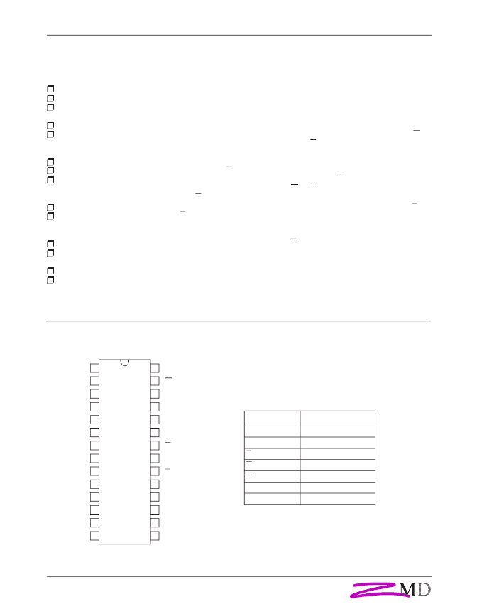
Pin Configuration
Top View
Signal Name
Signal Description
A0 - A14
DQ0 - DQ7
Address Inputs
Data In/Out
Chip Enable
Output Enable
Write Enable
Power Supply Voltage
Ground
E
G
W
VCC
VSS
Pin Description
1
A14
VCC
28
2
A12
W
27
4
A6
A8
25
5
A5
A9
24
3
A7
A13
26
6
A4
A11
23
7
A3
G
22
8
A2
A10
21
12
DQ1
DQ5
17
9
A1
E
DQ7
20
10
A0
19
11
DQ0
DQ6
18
13
DQ2
DQ4
16
14
VSS
DQ3
15
SOP
相關PDF資料 |
PDF描述 |
|---|---|
| U62H256SA55 | x8 SRAM |
| U62H256SK35 | Low power JFET dual operational amplifiers |
| U62H256SK55 | x8 SRAM |
| U62H824PC35 | Low power JFET quad operational amplifier |
| U62H824PK35 | x24 SRAM |
相關代理商/技術參數 |
參數描述 |
|---|---|
| U62H256SA55 | 制造商:未知廠家 制造商全稱:未知廠家 功能描述:x8 SRAM |
| U62H256SK35 | 制造商:未知廠家 制造商全稱:未知廠家 功能描述:x8 SRAM |
| U62H256SK55 | 制造商:未知廠家 制造商全稱:未知廠家 功能描述:x8 SRAM |
| U62H64 | 制造商:ZMD 制造商全稱:Zentrum Mikroelektronik Dresden AG 功能描述:AUTOMOTIVE FAST 8K X 8 SRAM |
| U62H64SA35 | 制造商:ZMD 制造商全稱:Zentrum Mikroelektronik Dresden AG 功能描述:AUTOMOTIVE FAST 8K X 8 SRAM |
發布緊急采購,3分鐘左右您將得到回復。