- 您現在的位置:買賣IC網 > PDF目錄382721 > UDA1360TS (NXP SEMICONDUCTORS) Low-voltage low-power stereo audio ADC PDF資料下載
參數資料
| 型號: | UDA1360TS |
| 廠商: | NXP SEMICONDUCTORS |
| 元件分類: | ADC |
| 英文描述: | Low-voltage low-power stereo audio ADC |
| 中文描述: | 2-CH 20-BIT DELTA-SIGMA ADC, SERIAL ACCESS, PDSO16 |
| 封裝: | 4.40 MM, PLASTIC, MO-152, SOT-369-1, SSOP-16 |
| 文件頁數: | 4/16頁 |
| 文件大小: | 84K |
| 代理商: | UDA1360TS |
2000 Feb 08
4
Philips Semiconductors
Preliminary specification
Low-voltage low-power stereo audio ADC
UDA1360TS
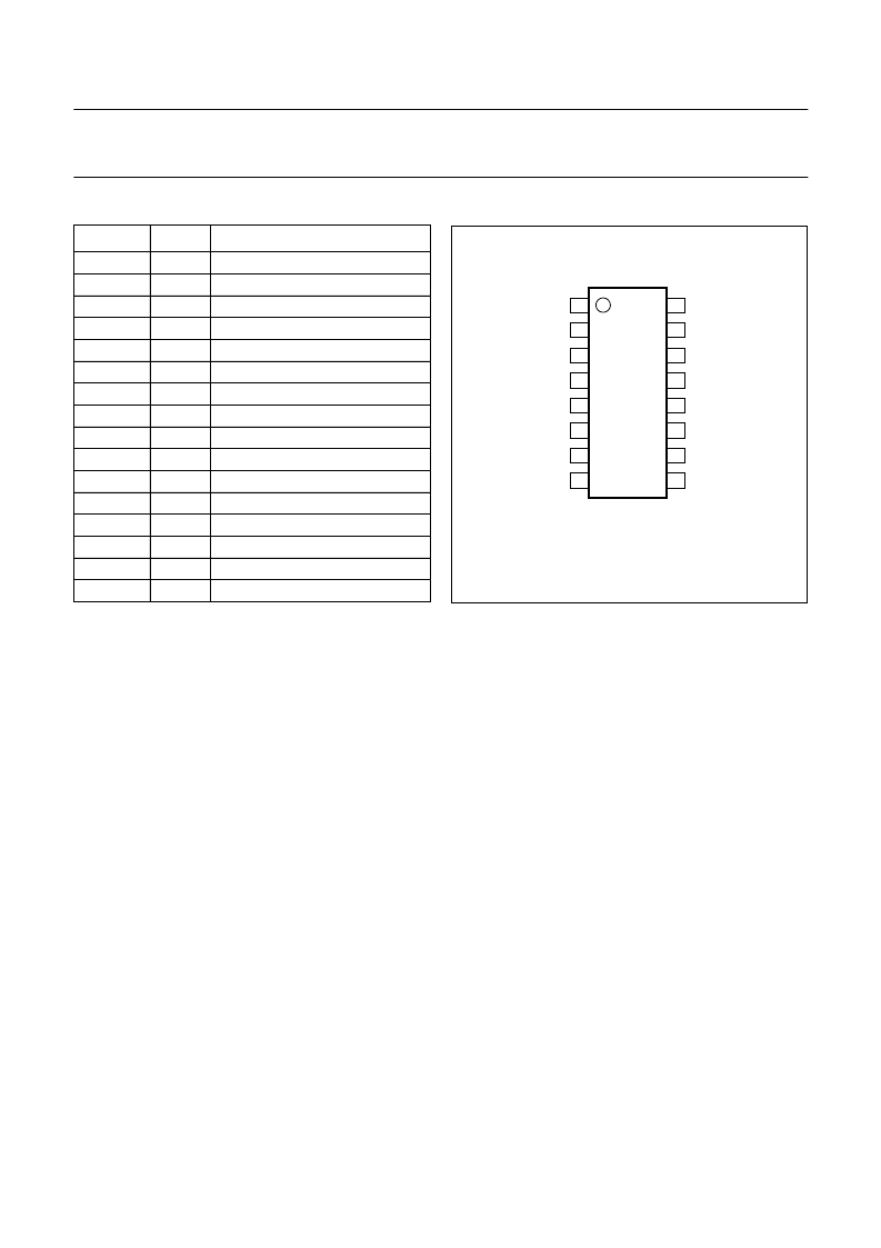
PINNING
SYMBOL
PIN
DESCRIPTION
VINL
V
ref
VINR
V
ref(n)
V
ref(p)
SFOR
PWON
SYSCLK
V
DDD
V
SSD
BCK
WS
DATAO
FSEL
V
SSA
V
DDA
1
2
3
4
5
6
7
8
9
10
11
12
13
14
15
16
left channel input
reference voltage
right channel input
ADC negative reference voltage
ADC positive reference voltage
data format selection input
power control input
system clock input 256 or 384f
s
digital supply voltage
digital ground
bit clock input
word selection input
data output
system clock frequency select
analog ground
analog supply voltage
Fig.2 Pin configuration.
handbook, halfpage
UDA1360TS
MGM968
1
2
3
4
5
6
7
8
16
15
14
13
12
11
10
9
VINL
Vref
VINR
Vref(n)
Vref(p)
SFOR
PWON
SYSCLK
VDDD
VSSD
BCK
WS
DATAO
FSEL
VSSA
VDDA
FUNCTIONAL DESCRIPTION
System clock
The UDA1360TS accommodates slave mode only, this
means that in all applications the system devices must
provide the system clock. The system frequency is
selectable via the static FSEL pin, and the system clock
must be locked in frequency to the digital interface input
signals.
The options are 256f
s
(FSEL = LOW) and 384f
s
(FSEL = HIGH). The sampling frequency range is
5 to 55 kHz.
The BCK clock can be up to 128f
s
, or in other words the
BCK frequency is 128 times the Word Select (WS)
frequency or less: f
BCK
≤
128
×
f
WS
.
Notes:
1.
The WS edge MUST fall on the negative edge of the
BCK at all times for proper operation of the digital I/O
data interface.
For MSB justified formats it is important to have a WS
signal with 50% duty factor.
2.
Analog-to-Digital Converter (ADC)
The stereo ADC of the UDA1360TS consists of two
3rd-order Sigma-Delta modulators. They have a modified
Ritchie-coder architecture in a differential switched
capacitor implementation. The over-sampling ratio is 128.
Input level
The overall system gain is proportional to V
DDA
. The 0 dB
input level is defined as that which gives a
1 dB FS digital
output(relativetothefull-scaleswing).Inaddition,aninput
gain switch is incorporated with the above definitions.
The UDA1360TS front-end is equipped with a selectable
0 or 6 dB gain, in order to supports 2 V (RMS) input using
a series resistor of 12 k
.
For the definition of the pin settings for 1 or 2 V (RMS)
mode given in Table 1, it is assumed that this resistor is
present as a default component.
If the 2 V (RMS) signal input is not needed, the external
resistor should not be used.
相關PDF資料 |
PDF描述 |
|---|---|
| UDA1361 | 96 kHz sampling 24-bit stereo audio ADC |
| UDA1380 | Stereo audio coder-decoder for MD, CD and MP3 |
| UDA1380TT | Stereo audio coder-decoder for MD, CD and MP3 |
| UDA1384 | Multichannel audio coder-decoder |
| UDA1384H | Multichannel audio coder-decoder |
相關代理商/技術參數 |
參數描述 |
|---|---|
| UDA1361 | 制造商:PHILIPS 制造商全稱:NXP Semiconductors 功能描述:96 kHz sampling 24-bit stereo audio ADC |
| UDA1361TS | 制造商:PHILIPS 制造商全稱:NXP Semiconductors 功能描述:96 kHz sampling 24-bit stereo audio ADC |
| UDA1361TS/N1 | 制造商:NXP Semiconductors 功能描述:ADC STEREO AUDIO 24BIT 16SSOP 制造商:NXP Semiconductors 功能描述:ADC, STEREO, AUDIO, 24BIT, 16SSOP |
| UDA1361TS/N1,112 | 功能描述:音頻模/數轉換器 IC ADC STEREO 7712 24BIT RoHS:否 制造商:Wolfson Microelectronics 轉換速率: 分辨率: ADC 輸入端數量: 工作電源電壓: 最大工作溫度: 最小工作溫度: 安裝風格: 封裝 / 箱體: 封裝: |
| UDA1361TS/N1,118 | 功能描述:音頻模/數轉換器 IC 24 BIT ADC RoHS:否 制造商:Wolfson Microelectronics 轉換速率: 分辨率: ADC 輸入端數量: 工作電源電壓: 最大工作溫度: 最小工作溫度: 安裝風格: 封裝 / 箱體: 封裝: |
發布緊急采購,3分鐘左右您將得到回復。