- 您現在的位置:買賣IC網 > PDF目錄383974 > UPA1759G (NEC Corp.) Switching N-channel power MOS FET industrial use PDF資料下載
參數資料
| 型號: | UPA1759G |
| 廠商: | NEC Corp. |
| 元件分類: | 功率晶體管 |
| 英文描述: | Switching N-channel power MOS FET industrial use |
| 中文描述: | N溝道 開關功率場效應晶體管 工業級 |
| 文件頁數: | 1/4頁 |
| 文件大小: | 38K |
| 代理商: | UPA1759G |
The information in this document is subject to change without notice. Before using this document, please
confirm that this is the latest version.
Not all devices/types available in every country. Please check with local NEC representative for
availability and additional information.
1999
MOS FIELD EFFECT TRANSISTOR
μ
PA1759
SWITCHING
N-CHANNEL POWER MOS FET
INDUSTRIAL USE
DATA SHEET
Document No.
Date Published
Printed in Japan
G13622EJ1V0DS00 (1st edition)
May 1999 NS CP(K)
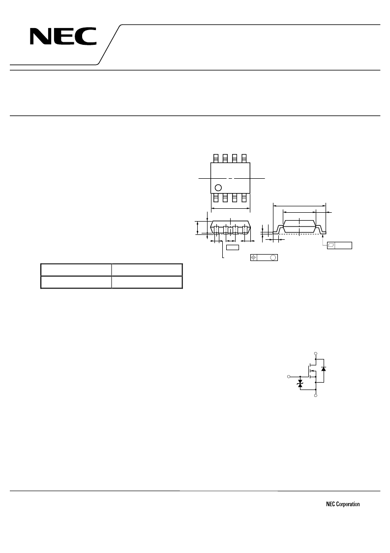
PACKAGE DRAWING (Unit : mm)
1.27
0.12 M
6.0 ±0.3
4.4
0.40
+0.10
0.78 Max.
0
1
1
0.8
0.5 ±0.2
0
+
–
5.37 Max.
0.10
1
4
8
5
1
2
7, 8
3
4
5, 6
; Source 1
; Gate 1
; Drain 1
; Source 2
; Gate 2
; Drain 2
EQUIVALENT CIRCUIT
(1/2 Circuit)
Source
Body
Diode
Gate
Protection
Diode
Gate
Drain
DESCRIPTION
This product is Dual N-channel MOS Field Effect
Transistor designed for DC/DC converters.
FEATURES
Dual chip type
Low on-resistance
R
DS(on)1
= 110 m
TYP. (V
GS
= 10
V, I
D
= 2.5
A)
R
DS(on)2
= 170 m
TYP. (V
GS
= 4
V, I
D
= 2.5
A)
Low input capacitance C
iss
= 190
pF TYP.
Built-in G-S protection diode
Small and surface mount package (Power SOP8)
ORDERING INFORMATION
PART NUMBER
PACKAGE
μ
PA1759G
Power SOP8
ABSOLUTE MAXIMUM RATINGS (T
A
= 25 °C, All terminals are connected.)
Drain to Source Voltage (V
GS
= 0)
Gate to Source Voltage (V
DS
= 0)
Drain Current (DC)
Drain Current (pulse)
Note1
Total Power Dissipation (1 unit)
Note2
Total Power Dissipation (2 unit)
Note2
Channel Temperature
Storage Temperature
Single Avalanche Current
Note3
Single Avalanche Energy
Note3
Notes 1.
PW
≤
10
μ
s, Duty cycle
≤
1 %
2.
Mounted on ceramic substrate of 1200 mm
2
x 1.7 mm
3.
Starting T
ch
= 25
°C, R
G
= 25
, V
GS
= 20
V
→
0 V
V
DSS
V
GSS
I
D(DC)
I
D(pulse)
P
T
P
T
T
ch
T
stg
I
AS
E
AS
60
±
20
±
5.0
±
20
1.7
2.0
150
V
V
A
A
W
W
°C
°C
A
mJ
–55 to + 150
2.5
0.625
Remark
The diode connected between the gate and source of the transistor serves as a protector against ESD.
When this device actually used, an additional protection circuit is externally required if a voltage exceeding
the rated voltage may be applied to this device.
相關PDF資料 |
PDF描述 |
|---|---|
| UPA1760 | Switching N-channel power MOS FET industrial use |
| UPA1763 | SWITCHING DUAL N-CHANNEL POWER MOS FET INDUSTRIAL USE |
| UPA1763G | SWITCHING DUAL N-CHANNEL POWER MOS FET INDUSTRIAL USE |
| UPA1774 | SWITCHING DUAL P-CHANNEL POWER MOSFET |
| UPA1774G | SWITCHING DUAL P-CHANNEL POWER MOSFET |
相關代理商/技術參數 |
參數描述 |
|---|---|
| UPA1760 | 制造商:NEC 制造商全稱:NEC 功能描述:SWITCHING N-CHANNEL POWER MOS FET INDUSTRIAL USE |
| UPA1760GE2 | 制造商:NEC 功能描述:New |
| UPA1763 | 制造商:NEC 制造商全稱:NEC 功能描述:SWITCHING DUAL N-CHANNEL POWER MOS FET INDUSTRIAL USE |
| UPA1763G | 制造商:NEC 制造商全稱:NEC 功能描述:SWITCHING DUAL N-CHANNEL POWER MOS FET INDUSTRIAL USE |
| UPA1763G-E1 | 制造商:Renesas Electronics Corporation 功能描述: |
發布緊急采購,3分鐘左右您將得到回復。