- 您現在的位置:買賣IC網 > PDF目錄16524 > XR16V2551IM-0B-EB (Exar Corporation)EVAL BOARD FOR V2551 48TQFP PDF資料下載
參數資料
| 型號: | XR16V2551IM-0B-EB |
| 廠商: | Exar Corporation |
| 文件頁數: | 1/49頁 |
| 文件大小: | 0K |
| 描述: | EVAL BOARD FOR V2551 48TQFP |
| 標準包裝: | 1 |
| 系列: | * |
當前第1頁第2頁第3頁第4頁第5頁第6頁第7頁第8頁第9頁第10頁第11頁第12頁第13頁第14頁第15頁第16頁第17頁第18頁第19頁第20頁第21頁第22頁第23頁第24頁第25頁第26頁第27頁第28頁第29頁第30頁第31頁第32頁第33頁第34頁第35頁第36頁第37頁第38頁第39頁第40頁第41頁第42頁第43頁第44頁第45頁第46頁第47頁第48頁第49頁
Exar Corporation 48720 Kato Road, Fremont CA, 94538 (510) 668-7000 FAX (510) 668-7017 www.exar.com
XR16V2551
HIGH PERFORMANCE DUART WITH 16-BYTE FIFO AND POWERSAVE FEATURE
DECEMBER 2011
REV. 1.0.3
GENERAL DESCRIPTION
The XR16V25511 (V2551) is a high performance dual
universal asynchronous receiver and transmitter
(UART) with 16 byte TX and RX FIFOs. The device
operates from 2.25 to 3.6 volts with 5 Volt tolerant
inputs and is pin-to-pin compatible to Exar’s
XR16V2651 and XR16L2551. The device includes 2
additional capabilities over the XR16V2550: Intel and
Motorola data bus selection and a “PowerSave”
mode to further reduce sleep current to a minimum
during sleep mode. It supports Exar’s enhanced
features of selectable FIFO trigger level, automatic
hardware (RTS/CTS) and software flow control, and a
complete modem interface. An internal loopback
capability allows system diagnostics. Independent
programmable fractional baud rate generators are
provided in each channel to select data rates up to 16
Mbps at 3.3 Volt and 4X sampling clock. The V2551
is available in 48-pin TQFP and 32-pin QFN
packages.
NOTE: 1 Covered by U.S. Patent #5,649,122
APPLICATIONS
Portable Appliances
Telecommunication Network Routers
Ethernet Network Routers
Cellular Data Devices
Factory Automation and Process Controls
FEATURES
2.25 to 3.6 Volt Operation
5 Volt Tolerant Inputs
Intel or Motorola Mode
Pin-to-pin compatible to Exar’s XR16V2651 and the
XR16L2551
Two independent UART channels
■ Register set identical to 16V2550
■ Data rate of up to 16 Mbps at 3.3 V, and 12.5
Mbps at 2.5 V with 4X sampling rate
■ Fractional Baud Rate Generator
■ Transmit and Receive FIFOs of 16 bytes
■ Selectable TX and RX FIFO Trigger Levels
■ Automatic Hardware (RTS/CTS) Flow Control
■ Automatic Software (Xon/Xoff) Flow Control
■ Wireless Infrared (IrDA 1.0) Encoder/Decoder
■ Automatic sleep mode with wake-up interrupt
■ Full modem interface
PowerSave Feature reduces sleep current to 15 A
Device Identification and Revision
Crystal oscillator (up to 32MHz) or external clock
(up to 64MHz) input
48-TQFP and 32-QFN packages
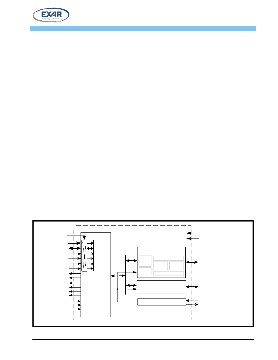
FIGURE 1. XR16V2551 BLOCK DIAGRAM
XTAL1
XTAL2
Crystal Osc/Buffer
TXA, RXA, DTRA#,
DSRA#, RTSA#,
DTSA#, CDA#, RIA#,
OP2A#
Intel or
Motorola
Data Bus
Interface
UART Channel A
16 Byte TX FIFO
16 Byte RX FIFO
BRG
IR
ENDEC
TX & RX
UART
Regs
2.25 to 3.6V VCC
GND
*5 Volt Tolerant Inputs
TXB, RXB, DTRB#,
DSRB#, RTSB#,
CTSB#, CDB#, RIB#,
OP2B#
UART Channel B
(same as Channel A)
A2:A0
D7:D0
CSA# (CS#)
16/68#
CSB# (A3)
INTA (IRQ#)
INTB (logic 0)
PwrSave
IOW# (R/W#)
IOR# (VCC)
Reset (Reset#)
CLKSEL
TXRDYA#
TXRDYB#
RXRDYA#
RXRDYB#
相關PDF資料 |
PDF描述 |
|---|---|
| UPS2W2R2MPD1TD | CAP ALUM 2.2UF 450V 20% RADIAL |
| GEM36DTBN | CONN EDGECARD 72POS R/A .156 SLD |
| UPJ2A270MPD6TD | CAP ALUM 27UF 100V 20% RADIAL |
| XR16V2550IM-0B-EB | EVAL BOARD FOR V2550 48TQFP |
| GCA22DCBH | CONN EDGECARD 44POS R/A .125 SLD |
相關代理商/技術參數 |
參數描述 |
|---|---|
| XR16V2551IM-F | 功能描述:UART 接口集成電路 UART RoHS:否 制造商:Texas Instruments 通道數量:2 數據速率:3 Mbps 電源電壓-最大:3.6 V 電源電壓-最小:2.7 V 電源電流:20 mA 最大工作溫度:+ 85 C 最小工作溫度:- 40 C 封裝 / 箱體:LQFP-48 封裝:Reel |
| XR16V2551IMTR-F | 制造商:Exar Corporation 功能描述:UART 2-CH 16Byte FIFO 2.5V/3.3V 48-Pin TQFP T/R 制造商:Exar Corporation 功能描述:XR16V2551IMTR-F |
| XR16V2552 | 制造商:EXAR 制造商全稱:EXAR 功能描述:HIGH PERFORMANCE DUART WITH 16-BYTE FIFO |
| XR16V2552_07 | 制造商:EXAR 制造商全稱:EXAR 功能描述:HIGH PERFORMANCE DUART WITH 16-BYTE FIFO |
| XR16V2552IJ | 制造商:Rochester Electronics LLC 功能描述: 制造商:Exar Corporation 功能描述: |
發布緊急采購,3分鐘左右您將得到回復。