- 您現在的位置:買賣IC網 > PDF目錄376459 > XRK39653 (Exar Corporation) 3.3V, 8-OUTPUT ZERO DELAY BUFFER PDF資料下載
參數資料
| 型號: | XRK39653 |
| 廠商: | Exar Corporation |
| 英文描述: | 3.3V, 8-OUTPUT ZERO DELAY BUFFER |
| 中文描述: | 3.3伏,8輸出零延時緩沖器 |
| 文件頁數: | 1/9頁 |
| 文件大小: | 76K |
| 代理商: | XRK39653 |
Exar
Corporation 48720 Kato Road, Fremont CA, 94538
(510) 668-7000
FAX (510) 668-7017
www.exar.com
xr
XRK39653
3.3V, 8-OUTPUT ZERO DELAY BUFFER
NOVEMBER 2006
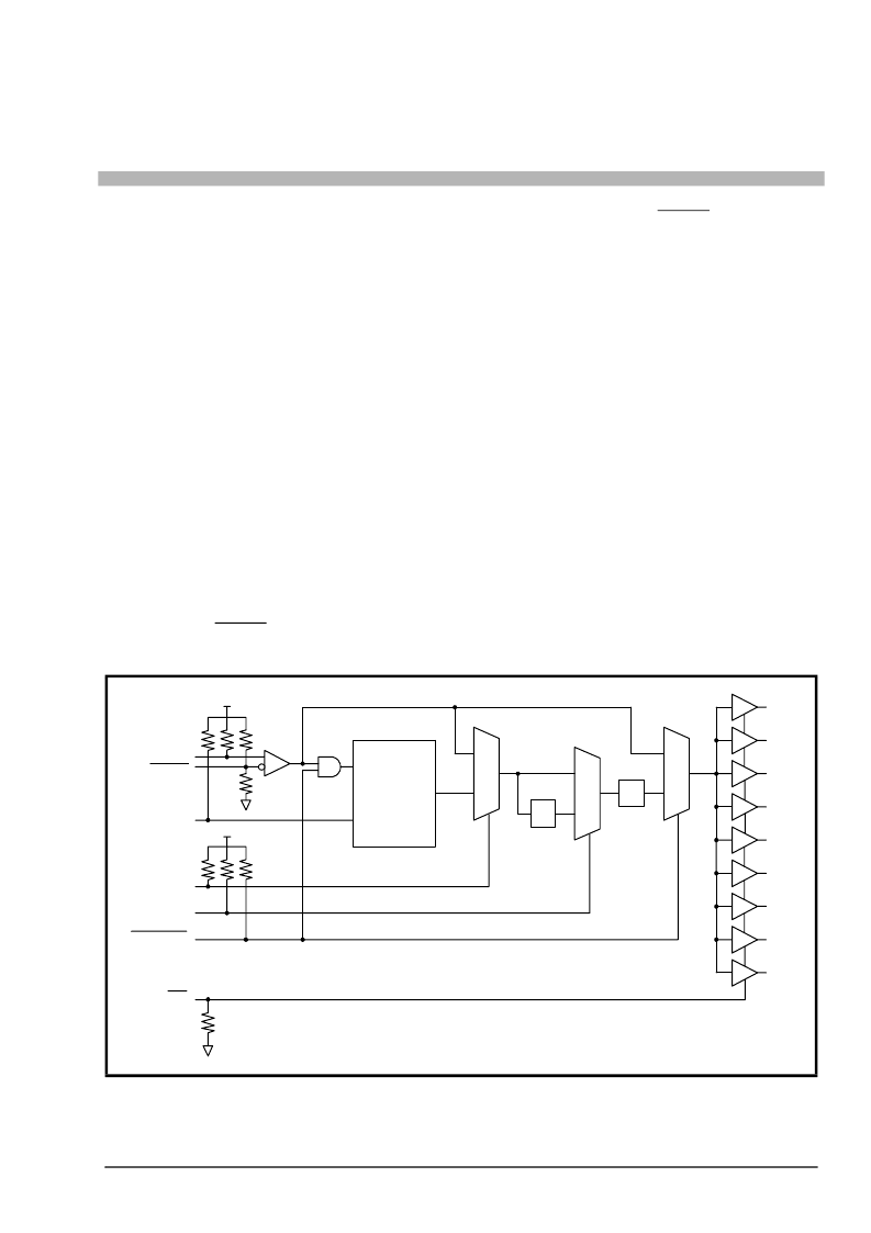
XRK39653 GENERAL DESCRIPTION
REV. 1.0.0
The XRK39653 is a low voltage high performance PLL
based zero delay buffer/clock generator designed for high
speed clock distribution applications. It provides 9 low
skew, low jitter outputs ideal for networking, computing and
telecom applications.
The PLL based design allows the 9 outputs (8 clock outputs
and 1 feedback output) to be phase aligned to the input ref-
erence clock. The outputs source LVCMOS compatible lev-
els and can drive 50
Ω
transmission lines. If series
termination is used, each output can drive up to 2 lines pro-
viding effectively a fanout of 1:16. The XRK39653’s refer-
ence input accepts a LVPECL clock source.
For normal operation (PLL used to source the outputs), the
feedback output (QFB) is connected to the feedback input
(FB_IN). The VCO range of operation is 200 to 500MHz.
This means that the input/output ranges are determined by
the divider setting. If ÷4 is used, the input/output range is 50
to 125MHz (high range), if ÷8 is used the input/output range
is 25 to 62.5MHz (low range).
For testing purposes two PLL bypass modes are provided.
The first simply replaces the PLL output with the reference
clock (PLL_EN=0, BYPASS=1). The dividers are still in
use. The second is a full bypass mode that has the PLL
and divider operation removed (BYPASS=0). In this mode
the reference clock directly sources the outputs drivers.
FEATURES
8 LVCMOS Clock Outputs
1 Feedback Output
LVPECL reference clock input
25-125 MHz input/output frequency range
■
Input/Output range (
÷4): 50-125MHz
■
Input/Output range (
÷8): 25-62.5MHz
150ps max output to output skew
Two bypass test mode options
Fully Integrated PLL
3.3V Operation
Pin compatible with MPC9653
Industrial temp range:
-40°C to +85°C
32-Lead TQFP Packaging
F
IGURE
1. B
LOCK
D
IAGRAM
OF
THE
XRK39653
PLL
FB
Ref
1
0
1
0
1
0
FB_IN
PLL_EN
OE
PECL
PECL
Q5
Q6
Q7
QFB
2
÷
4
÷
Q4
Q0
Q1
Q2
Q3
VCO_SEL
BYPASS
VDD
VDD
相關PDF資料 |
PDF描述 |
|---|---|
| XRK39653CQ | 3.3V, 8-OUTPUT ZERO DELAY BUFFER |
| XRK39653IQ | 3.3V, 8-OUTPUT ZERO DELAY BUFFER |
| XRK39653IQ-F | 3.3V, 8-OUTPUT ZERO DELAY BUFFER |
| XRK39910 | 3.3V LOW SKEW PLL CLOCK DRIVER |
| XRK39910CD-2 | 3.3V LOW SKEW PLL CLOCK DRIVER |
相關代理商/技術參數 |
參數描述 |
|---|---|
| XRK39653_0611 | 制造商:EXAR 制造商全稱:EXAR 功能描述:3.3V, 8-OUTPUT ZERO DELAY BUFFER |
| XRK39653CQ | 制造商:EXAR 制造商全稱:EXAR 功能描述:3.3V, 8-OUTPUT ZERO DELAY BUFFER |
| XRK39653IQ | 制造商:EXAR 制造商全稱:EXAR 功能描述:3.3V, 8-OUTPUT ZERO DELAY BUFFER |
| XRK39653IQ-F | 制造商:EXAR 制造商全稱:EXAR 功能描述:3.3V, 8-OUTPUT ZERO DELAY BUFFER |
| XRK39910 | 制造商:EXAR 制造商全稱:EXAR 功能描述:3.3V LOW SKEW PLL CLOCK DRIVER |
發布緊急采購,3分鐘左右您將得到回復。