- 您現(xiàn)在的位置:買(mǎi)賣(mài)IC網(wǎng) > PDF目錄382753 > Z9974CA DIODE TVS 16V 500W BI-DIR PDF資料下載
參數(shù)資料
| 型號(hào): | Z9974CA |
| 英文描述: | DIODE TVS 16V 500W BI-DIR |
| 中文描述: | 共14名分布式輸出時(shí)鐘驅(qū)動(dòng)器| TQFP封裝| 52PIN |塑料 |
| 文件頁(yè)數(shù): | 1/9頁(yè) |
| 文件大小: | 62K |
| 代理商: | Z9974CA |
3.3V, 125MHz, Multi-Output Zero Delay Buffer
Cypress Semiconductor Corporation
525 Los Coches St.
Milpitas, CA 95035. Tel: 408-263-6300, Fax: 408-263-6571
http://www.cypress.com
Document#: 38-07090 Rev. *A
06/18/2001
Page 1 of 9
Z9974
Product Features
Output Frequency up to 125MHz
Supports Power PC
TM
, and Pentium
TM
Processors
15 Clock Output: Frequency Configurable
Two Reference Clock Inputs for Dynamic Toggling
Output Tri-State Control
Spread Spectrum Compatible
3.3V Power Supply
Pin Compatible with MPC974
Industrial Temp. Range: -40°C to +85°C
52 Pin TQFP Package
Product Description
The Z9974 is a low cost 3.3V zero delay clock driver for
high speed signal buffering and redistribution.
It provides the designer with the flexibility of selecting
various Output/Input Frequency ratios selected by fsela,
fselb, fselc, fselFB(0:1), and VCO_sel input settings.
The Z9974 integrates PLL technology for Zero delay
propagation from Input to Output. The PLL feedback is
externally available for propagation delay tuning and
divide ratio alternatives as per table 1.
The Z9974 has three banks of outputs with independent
divider stages. These dividers allow the banks to have
different frequencies as per table 2.
TCLK0 and TCLK1 one are selectable input reference
clocks and may be toggled dynamically during operation
to provide modulation and phase shifting designs.
This device includes a Master Reset signal, which
disables the outputs into Tristate (Hi-Z) mode, and reset
all internal digital circuitry (excluding the PLL).
An Output Enable, OE, input pin is available for shutting
Qa(0:4), Qb(0:4), and Qc(0:3) outputs in a low state. All
outputs are held low with input clock turned off.
Feedback Ratio Selection Table
Inputs
VCO_Sel
fselFB0
0
0
0
0
0
1
0
1
1
0
1
0
1
1
1
1
Outputs
QFB
VCO/8
VCO/12
VCO/16
VCO/24
VCO/16
VCO/24
VCO/32
VCO/48
fselFB1
0
1
0
1
0
1
0
1
Table 1
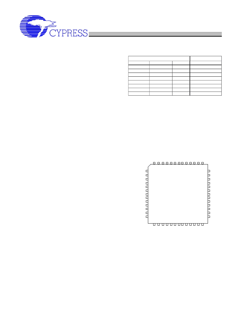
Pin Configuration
VSSA
MR#
OE
fselb
fselc
PLL_EN
fsela
TClk_Sel
TClk0
TClk1
NC
VDDI
VDDA
V
Q
V
Q
V
Q
f
V
Q
V
Q
V
f
Q
V
N
V
Q
V
Q
V
Q
V
Q
V
V
VSSb
QB1
VDDb
Qb2
VSSb
Qb3
VDDb
Qb4
FB_IN
VSSFB
QFB
VDDFB
NC
1
2
3
4
5
6
7
8
9
10
11
12
13
39
38
37
36
35
34
33
32
31
30
29
28
27
14 15 16 17 18 19 20 21 22 23 24 25 26
52 51 50 49 48 47 46 45 44 43 42 41 40
Z9974
相關(guān)PDF資料 |
PDF描述 |
|---|---|
| ZAD1025 | DIODE TVS 5.0V 500W UNI-DIR |
| ZAD1030 | Converter IC |
| ZAD1202 | SCR Thyristor; Thyristor Type:Standard Gate; Peak Repetitive Off-State Voltage, Vdrm:1000V; On-State RMS Current, IT(rms):8A; Peak Non Repetitive Surge Current, Itsm:100A; Gate Trigger Current Max, Igt:15uA RoHS Compliant: Yes |
| ZAD2736-2BU | DIODE TVS 180V 400W BIDIR 5% SMA |
| ZAD2744 | Converter IC |
相關(guān)代理商/技術(shù)參數(shù) |
參數(shù)描述 |
|---|---|
| Z9975 | 制造商:CYPRESS 制造商全稱:Cypress Semiconductor 功能描述:3.3V, 150MHz, Multi-Output Zero Delay Buffer |
| Z9975CA | 制造商:CYPRESS 制造商全稱:Cypress Semiconductor 功能描述:3.3V, 150MHz, Multi-Output Zero Delay Buffer |
| Z99SC61235 | 制造商:MINI CIRCU 功能描述:NEW |
| ZA000260R | 制造商:Denon Electronics 功能描述:DENON AM ANTENNA 116010001004S |
| ZA00106FSC | 制造商:Zilog Inc 功能描述: |
發(fā)布緊急采購(gòu),3分鐘左右您將得到回復(fù)。