- 您現(xiàn)在的位置:買賣IC網(wǎng) > PDF目錄68800 > 5962-9864601QEX (ANALOG DEVICES INC) LOG OR ANTILOG AMPLIFIER, 395 MHz BAND WIDTH, CDIP16 PDF資料下載
參數(shù)資料
| 型號(hào): | 5962-9864601QEX |
| 廠商: | ANALOG DEVICES INC |
| 元件分類: | 模擬運(yùn)算功能 |
| 英文描述: | LOG OR ANTILOG AMPLIFIER, 395 MHz BAND WIDTH, CDIP16 |
| 封裝: | SIDE BRAZED, CERAMIC, DIP-16 |
| 文件頁數(shù): | 15/16頁 |
| 文件大小: | 397K |
| 代理商: | 5962-9864601QEX |
REV. A
AD8306
–8–
voltage sensitivity. Most interfaces have additional small junc-
tion capacitances associated with them, due to active devices or
ESD protection; these may be neither accurate nor stable.
Component numbering in each of these interface diagrams is
local.
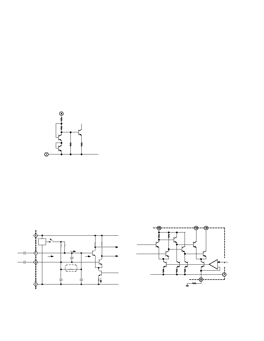
Enable Interface
The chip-enable interface is shown in Figure 20. The current in
R1 controls the turn-on and turn-off states of the band-gap
reference and the bias generator, and is a maximum of 100
A
when Pin 8 is taken to 5 V. Left unconnected, or at any voltage
below 1 V, the AD8306 will be disabled, when it consumes a
sleep current of much less than 1
A (leakage currents only); when
tied to the supply, or any voltage above 2 V, it will be fully enabled.
The internal bias circuitry requires approximately 300 ns for
either OFF or ON, while a delay of some 6
s is required for the
supply current to fall below 10
A.
1.3k
50k
4k
COMM
ENBL
R1
60k
TO BIAS
ENABLE
Figure 20. Enable Interface
Input Interface
Figure 21 shows the essentials of the signal input interface. The
parasitic capacitances to ground are labeled CP; the differential
input capacitance, CD, mainly due to the diffusion capacitance
of Q1 and Q2. In most applications both input pins are ac-
coupled. The switch S closes when Enable is asserted. When
disabled, the inputs float, bias current IE is shut off, and the
coupling capacitors remain charged. If the log amp is disabled
for long periods, small leakage currents will discharge these
capacitors. If they are poorly matched, charging currents at
power-up can generate a transient input voltage which may
block the lower reaches of the dynamic range until it has be-
come much less than the signal.
RIN = 1k
CC
SIGNAL
INPUT
INLO
INHI
VPS1
COMM
1.78V
3.65k
1.725V
CD
2.5pF
IB = 15mA
(TOP-END
DETECTORS)
CP
RIN = 3k
Q1
20e
Q2
20e
130
3.4mA
PTAT
GAIN BIAS
1.26V
67
TO STAGES
1 THRU 5
TO 2ND
STAGE
S
2.6k
Figure 21. Signal Input Interface
In most applications, the input signal will be single-sided, and
may be applied to either Pin 4 or 5, with the remaining pin ac-
coupled to ground. Under these conditions, the largest input
signal that can be handled is –3 dBV (sine amplitude of 1 V)
when operating from a 3 V supply; a +3 dBV input may be
handled using a supply of 4.5 V or greater. When using a fully-
balanced drive, the +3 dBV level may be achieved for the sup-
plies down to 2.7 V and +9 dBV using >4.5 V. For frequencies
in the range 10 MHz to 200 MHz these high drive levels are
easily achieved using a matching network. Using such a net-
work, having an inductor at the input, the input transient is
eliminated.
Limiter Output Interface
The simplified limiter output stage is shown in Figure 22. The
bias for this stage is provided by a temperature-stable reference
voltage of nominally 400 mV which is forced across the exter-
nal resistor RLIM connected from Pin 9 (LMDR, or limiter
drive) by a special op amp buffer stage. The biasing scheme
also introduces a slight “l(fā)ift” to this voltage to compensate for
the finite current gain of the current source Q3 and the output
transistors Q1 and Q2. A maximum current of 10 mA is per-
missible (RLIM = 40 ). In special applications, it may be desir-
able to modulate the bias current; an example of this is provided
in the Applications section. Note that while the bias currents are
temperature stable, the ac gain of this stage will vary with tem-
perature, by –6 dB over a 120
°C range.
A pair of supply and temperature stable complementary cur-
rents is generated at the differential output LMHI and LMLO
(Pins 12 and 13), having a square wave form with rise and fall
times of typically 0.6 ns, when load resistors of 50
are used.
The voltage at these output pins may swing to 1.2 V below the
supply voltage applied to VPS2 (Pin 15).
Because of the very high gain bandwidth product of this ampli-
fier considerable care must be exercised in using the limiter
outputs. The minimum necessary bias current and voltage
swings should be used. These outputs are best utilized in a
fully-differential mode. A flux-coupled transformer, a balun, or
an output matching network can be selected to transform these
voltages to a single-sided form. Equal load resistors are recom-
mended, even when only one output pin is used, and these
should always be returned to the same well decoupled node on
the PC board. When the AD8306 is used only to generate an
RSSI output, the limiter should be completely disabled by
omitting RLIM and strapping LMHI and LMLO to VPS2.
OA
VPS2
LMHI
LMLO
COM1
LMDR
RLIM
2.6k
1.3k
Q1
4e
Q2
4e
Q3
1.3k
FROM FINAL
LIMITER STAGE
400mV
ZERO-TC
Figure 22. Limiter Output Interface
RSSI Output Interface
The outputs from the ten detectors are differential currents,
having an average value that is dependent on the signal input
level, plus a fluctuation at twice the input frequency. The cur-
rents are summed at the internal nodes LGP and LGN shown
in Figure 23. A further current IT is added to LGP, to position
相關(guān)PDF資料 |
PDF描述 |
|---|---|
| 5962-9959101QPA | 3-CHANNEL POWER SUPPLY SUPPORT CKT, CDIP8 |
| 5962-9959101Q2A | 3-CHANNEL POWER SUPPLY SUPPORT CKT, CQCC20 |
| 5962F0623701V9A | OP-AMP, 500 uV OFFSET-MAX, 7.5 MHz BAND WIDTH, UUC |
| 5962F0623701VXC | OP-AMP, 500 uV OFFSET-MAX, 7.5 MHz BAND WIDTH, CDFP8 |
| 5962F9553602VPA | OP-AMP, 7000 uV OFFSET-MAX, 200 MHz BAND WIDTH, CDIP8 |
相關(guān)代理商/技術(shù)參數(shù) |
參數(shù)描述 |
|---|---|
| 5962-9865101QFA | 功能描述:LVDS 接口集成電路 RoHS:否 制造商:Texas Instruments 激勵(lì)器數(shù)量:4 接收機(jī)數(shù)量:4 數(shù)據(jù)速率:155.5 Mbps 工作電源電壓:5 V 最大功率耗散:1025 mW 最大工作溫度:+ 85 C 封裝 / 箱體:SOIC-16 Narrow 封裝:Reel |
| 5962-9865101QXA | 制造商:Texas Instruments 功能描述: |
| 5962-9865201QFA | 功能描述:LVDS 接口集成電路 RoHS:否 制造商:Texas Instruments 激勵(lì)器數(shù)量:4 接收機(jī)數(shù)量:4 數(shù)據(jù)速率:155.5 Mbps 工作電源電壓:5 V 最大功率耗散:1025 mW 最大工作溫度:+ 85 C 封裝 / 箱體:SOIC-16 Narrow 封裝:Reel |
| 5962-9865501QJA | 制造商:Texas Instruments 功能描述:Latch/Decoder/Demultiplexer Single 4-to-16 24-Pin CDIP Tube |
| 5962-9865901HXA | 制造商:Analog Devices 功能描述:ADC Dual Pipelined 65Msps 12-bit Parallel 68-Pin LCCC 制造商:Rochester Electronics LLC 功能描述:- Bulk |
發(fā)布緊急采購,3分鐘左右您將得到回復(fù)。