- 您現在的位置:買賣IC網 > PDF目錄369233 > 6MBI75S-060 (FUJI ELECTRIC CO LTD) IGBT Module PDF資料下載
參數資料
| 型號: | 6MBI75S-060 |
| 廠商: | FUJI ELECTRIC CO LTD |
| 元件分類: | IGBT 晶體管 |
| 英文描述: | IGBT Module |
| 中文描述: | 75 A, 600 V, N-CHANNEL IGBT |
| 封裝: | MODULE-39 |
| 文件頁數: | 4/13頁 |
| 文件大小: | 529K |
| 代理商: | 6MBI75S-060 |
H04-004-03
13
MS5F5326
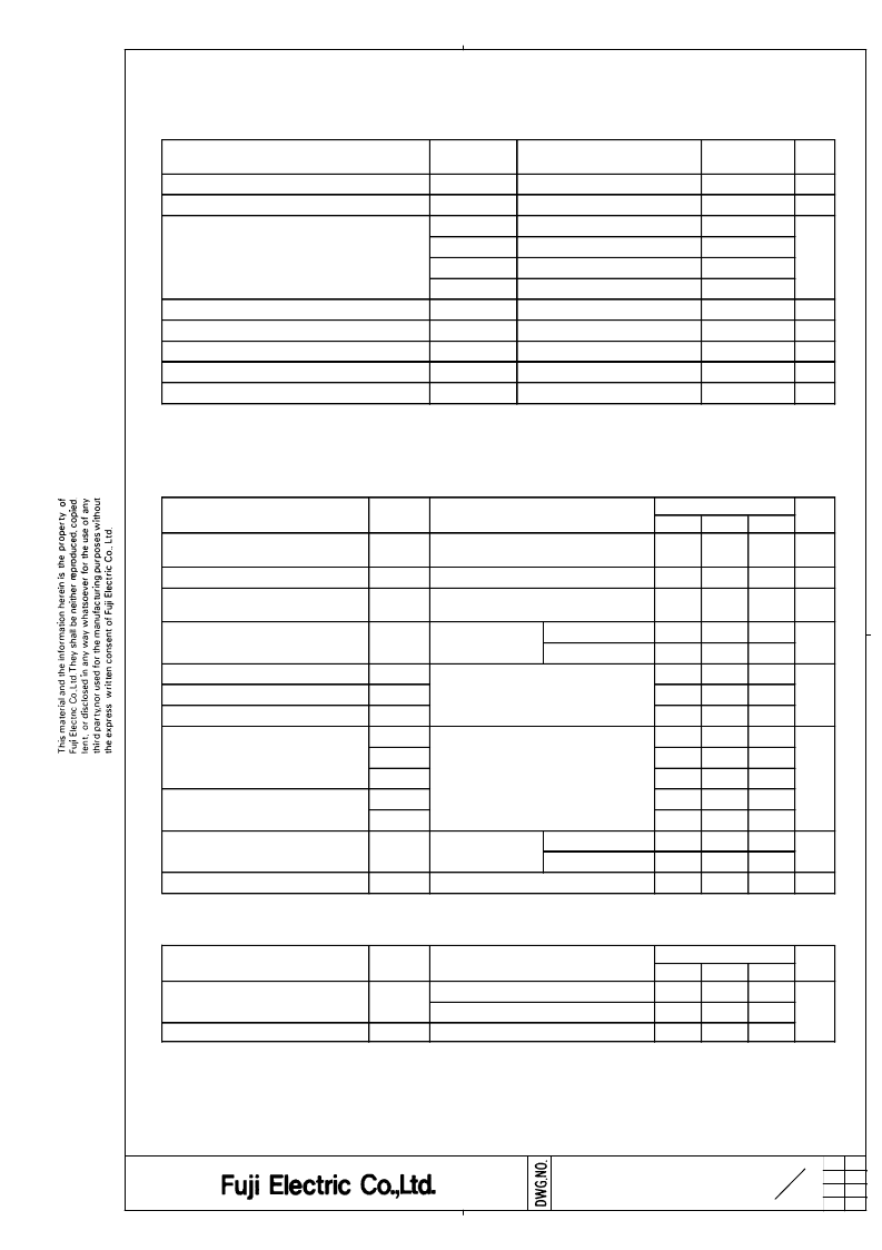
3. Absolute Maximum Ratings ( at Tc= 25C unless otherwise specified
)
Items
Symbols
Conditions
Maximum
Ratings
600
Units
Collector-Emitter voltage
V
CES
V
GES
V
Gate-Emitter voltage
+-20
75
V
Ic
Continuous
Collector current
Ic pulse
-Ic
1ms
150
A
75
-Ic pulse
Pc
1ms
1 device
150
300
Collector Power Dissipation
W
Junction temperature
Tj
150
C
Storage temperature
Isolation voltage
(*1)
Mounting Screw Torque
(*2)
(*1) All terminals should be connected together when isolation test will be done.
(*2) Recommendable Value : 2.5~3.5 Nm (M5)
Tstg
Viso
-40~ +125
2500
C
V
AC : 1min.
3.5
Nm
4. Electrical characteristics ( at Tj= 25C unless otherwise specified)
Characteristics
min.
typ.
Items
Symbols
Conditions
Max.
Units
Zero gate voltage
Collector current
Gate-Emitter leakage current
Gate-Emitter
threshold voltage
Collector-Emitter
saturation voltage
I
CES
V
GE
=
0 V,
V
CE
=
600 V
-
-
1.0
mA
I
GES
V
CE
=
0 V,
V
GE
=
+-20 V
-
-
200
nA
V
GE(th)
V
CE
=
20 V,
Ic =
75 mA
5.5
7.8
8.5
V
V
CE(sat)
V
GE
=
15 V
75 A
Tj =
Tj =
25 C
125 C
-
2.10
2.3
2.55
V
Ic =
-
-
Input capacitance
Cies
V
GE
=
V
CE
=
f=
0 V
-
7500
-
Output capacitance
Reverse transfer capacitance
Coes
Cres
10 V
1 MHz
-
1200
825
-
pF
-
-
ton
Vcc =
300 V
-
0.45
1.2
Turn-on time
tr
tr
(i)
toff
Ic =
V
GE
=
R
G
=
75 A
+-15 V
-
0.25
0.08
0.6
-
-
us
Turn-off time
33 ohm
-
0.40
1.0
tf
-
0.05
2.00
0.35
2.7
Forward on voltage
V
F
I
F
=
75 A
Tj =
25 C
-
V
Tj =
125 C
-
1.9
-
0.3
Reverse recovery time
trr
IF =
75 A
-
-
us
5. Thermal resistance characteristics
Characteristics
min.
typ.
Items
Symbols
Conditions
Max.
0.42
Units
Thermal resistance
R
th(j-c)
IGBT
-
-
(1 device)
FWD
with Thermal Compound
(*)
-
-
0.05
0.90
C/W
Contact Thermal resistance
* This is the value which is defined mounting on the additional cooling fin with thermal compound.
R
th(c-f)
-
-
4
相關PDF資料 |
PDF描述 |
|---|---|
| 6MBI75S-120-01 | IGBT Module |
| 6MBI75U2A-060 | IGBT module |
| 6MBI75U4A-120 | IGBT MODULE |
| 6MBI8F-120 | IGBT(1200V 8A) |
| 6MBI8L-120 | IGBT(1200V 8A) |
相關代理商/技術參數 |
參數描述 |
|---|---|
| 6MBI75S-120 | 制造商:FUJI 制造商全稱:Fuji Electric 功能描述:IGBT MODULE |
| 6MBI75S-120_10 | 制造商:FUJI 制造商全稱:Fuji Electric 功能描述:IGBT MODULE |
| 6MBI75S-120-01 | 制造商:FUJI 制造商全稱:Fuji Electric 功能描述:IGBT Module |
| 6MBI75S-120-50 | 制造商:Fuji Electric 功能描述:6-PACK IGBT MODULE 75A 1200V NPT |
| 6MBI75S-140 | 制造商:FUJI 制造商全稱:Fuji Electric 功能描述:IGBT Module |
發布緊急采購,3分鐘左右您將得到回復。