- 您現在的位置:買賣IC網 > PDF目錄36337 > 935261222557 (NXP SEMICONDUCTORS) SPECIALTY CONSUMER CIRCUIT, PQFP64 PDF資料下載
參數資料
| 型號: | 935261222557 |
| 廠商: | NXP SEMICONDUCTORS |
| 元件分類: | 消費家電 |
| 英文描述: | SPECIALTY CONSUMER CIRCUIT, PQFP64 |
| 封裝: | PLASTIC, SOT-319, QFP-64 |
| 文件頁數: | 9/36頁 |
| 文件大小: | 203K |
| 代理商: | 935261222557 |
第1頁第2頁第3頁第4頁第5頁第6頁第7頁第8頁當前第9頁第10頁第11頁第12頁第13頁第14頁第15頁第16頁第17頁第18頁第19頁第20頁第21頁第22頁第23頁第24頁第25頁第26頁第27頁第28頁第29頁第30頁第31頁第32頁第33頁第34頁第35頁第36頁
1999 Jun 14
17
Philips Semiconductors
Preliminary specication
ATSC 8-VSB demodulator and decoder
TDA8960
ADDRESSING THE DEVICE
Addressing the VSB demodulator over the system the
I2C-bus requires that the 7-bit slave address (A6 to A0) of
the device is sent over the bus in accordance with the
protocols, together with the R/W bit equal to logic 1 or 0 to
write or read data respectively.
The slave address of the device is shown in Table 9. Bits
0 to 6 are predefined, but bits 0 and 1 can be set using the
external pins A0 and A1.
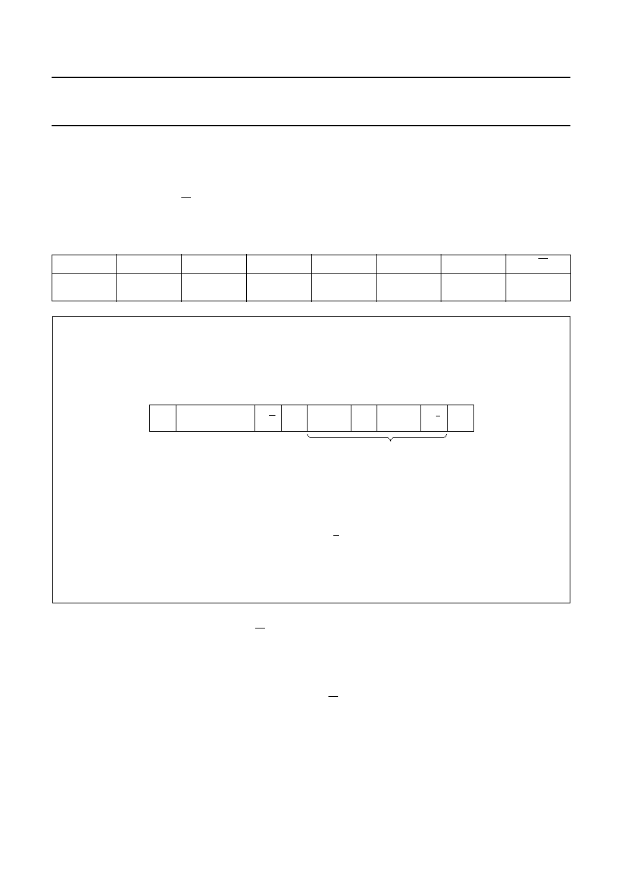
Table 9
Slave address
A6
A5
A4
A3
A2
A1
A0
R/W
00011
A1
A0
0 = write
1 = read
Fig.8 A master-transmitter addresses a slave receiver with a 7-bit address (write access).
(5) A = acknowledge (SDA LOW)
(6) A = not acknowledge (SDA HIGH)
(7) P = STOP condition
(8) Data transferred (n bytes + acknowledge).
(1) From master to slave
(2) S = START condition
(3) Logic 0 (write)
(4) From slave to master
handbook, full pagewidth
MGR607
S
A
DATA
A
(8)
DATA
P
SLAVE ADDRESS
(1)(2)
(1)(3)
(4)(5)
(1)
(4)(5)
(4)(5)(6)
(1)
(1)(7)
(1)
R/W
A/A
A write operation is shown in Fig.8. After the START
condition, the slave address followed by the R/W bit is
transmitted. The receiver, the TDA8960, sends an
acknowledge and the transmitter starts sending the
register values. After each received byte, the TDA8960
sends an acknowledge. The transfer stops if the TDA8960
does not acknowledge the transfer and/or the master
sends a STOP condition.
If register 08H has to be written to, eight consecutive bytes
are written. The first corresponds to register 01H, the
second to 02H and so on. The TDA8960 will
auto-increment the accessed address automatically. Up to
ten consecutive addresses can be written.
In Table 11 the default values are given for a number of
reserved addresses and reserved bits of certain
addresses. These correct default values have to be written
in order to prevent unexpected behaviour of the IC.
Figure 9 shows a read operation. The master sends a
START condition followed by the slave address and the
R/W bit is set to logic 1. The slave returns an acknowledge
followed by the value of the first address. The master
sends another acknowledge and the next value of the
address is returned. If the master transmits a STOP
condition after the acknowledge, the transfer is stopped.
Up to three consecutive addressed (00H to 03H) can be
read.
相關PDF資料 |
PDF描述 |
|---|---|
| 935261242118 | SERIAL INPUT LOADING, 20-BIT DAC, PDSO16 |
| 935261242112 | SERIAL INPUT LOADING, 20-BIT DAC, PDSO16 |
| 935261315112 | 2 CHANNEL(S), VOLUME CONTROL CIRCUIT, PDSO20 |
| 935261315118 | 2 CHANNEL(S), VOLUME CONTROL CIRCUIT, PDSO20 |
| 935261316112 | 2 CHANNEL(S), VOLUME CONTROL CIRCUIT, PDSO20 |
相關代理商/技術參數 |
參數描述 |
|---|---|
| 935262025112 | 制造商:NXP Semiconductors 功能描述:SUB ONLY IC |
| 935262217118 | 制造商:NXP Semiconductors 功能描述:Real Time Clock Serial 8-Pin SO T/R |
| 935264217557 | 制造商:NXP Semiconductors 功能描述:SUB ONLY IC |
| 935267356112 | 制造商:NXP Semiconductors 功能描述:IC TEA1507PN |
| 935268081112 | 制造商:NXP Semiconductors 功能描述:SUB ONLY IC |
發布緊急采購,3分鐘左右您將得到回復。