- 您現(xiàn)在的位置:買賣IC網(wǎng) > PDF目錄36340 > 935270456518 (NXP SEMICONDUCTORS) 4-CHANNEL POWER SUPPLY SUPPORT CKT, PDSO20 PDF資料下載
參數(shù)資料
| 型號(hào): | 935270456518 |
| 廠商: | NXP SEMICONDUCTORS |
| 元件分類: | 電源管理 |
| 英文描述: | 4-CHANNEL POWER SUPPLY SUPPORT CKT, PDSO20 |
| 封裝: | 4.40 MM, PLASTIC, SOT-163, TSOP-20 |
| 文件頁(yè)數(shù): | 4/10頁(yè) |
| 文件大小: | 158K |
| 代理商: | 935270456518 |
Philips Semiconductors
Product data
NE57605
Lithium-ion battery protector for
3 or 4 cell battery packs
2001 Oct 03
3
ORDERING INFORMATION
TYPE NUMBER
PACKAGE
TEMPERATURE
TYPE NUMBER
NAME
DESCRIPTION
RANGE
NE57605CD
TSOP-20A
plastic thin shrink small outline package; 20 leads; body width 4.4 mm
–20 to +70
°C
Part number marking
Each device is marked with a four letter code. The first three letters
in the top line of markings designate the product. The fourth letter,
represented by “x”, is a date code. The remaining markings are
manufacturing codes.
Part Number
Marking
NE57605CD
ALZx
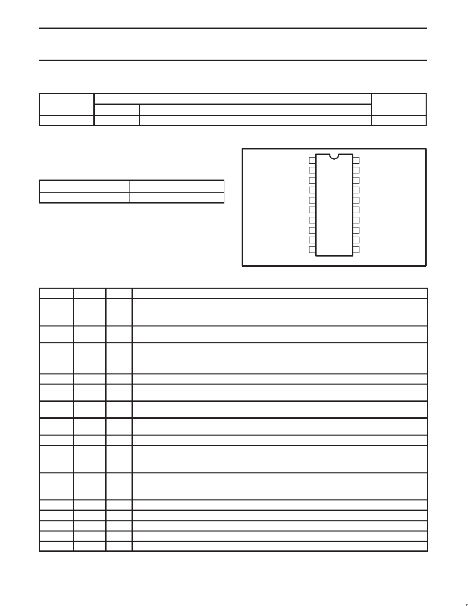
PIN CONFIGURATION
1
2
3
4
5
6
7
8
9
11
12
13
14
15
16
17
18
19
20
CF
NC
CS
NC
DF
NC
CDLY(UV)
CDLY(OC)
CDLY(OV)
GND
VCC
NC
VC4
VC3
VC2
VC1
NC
CON
SEL
10
SL01583
Figure 2. Pin configuration.
PIN DESCRIPTION
PIN
SYMBOL
I/O
DESCRIPTION
1
CF
Output
Overcharge detection output pin.
NPNTr open collector output.
Normal: high impedance.
Overcharge: LOW.
2, 4, 6,
12, 14, 19
NC
–
Not Connected.
3
CS
Input
Overcurrent detection pin. Monitors load current equivalently by the voltage drop between discharge
control FET source and drain, and makes DF pin HIGH when the voltage goes below overcurrent detection
voltage, turning off discharge control FET. After overcurrent detection, current flows from this pin and when
there is a light load, overcurrent mode is released. This function does not operate in overdischarge mode.
5
DF
Output
Discharge control FET (P-ch) drive pin. Normal: LOW. Overdischarge: HIGH.
7
CDLY(UV)
Input
Overdischarge detection dead time setting pin. Dead time can be set by connecting a capacitor between
CDLY(UV) pin and ground.
8
CDLY(OC)
Input
Overcurrent detection dead time setting pin. Dead time can be set by connecting a capacitor between
CDLY(OC) pin and ground.
9
CDLY(OV)
Input
Overcharge detection dead time setting pin. Dead time can be set by connecting a capacitor between
CDLY(OV) pin and ground.
10
GND
–
Ground pin.
11
SEL
Input
3/4 cell selection pin.
SEL pin = GND: 3 cell (Connect VC1 to GND).
SEL pin = VCC: 4 cell.
13
CON
Input
Discharge FET ON/OFF pin.
CON pin LOW; DF pin LOW (Normal mode).
CON pin HIGH; DF pin HIGH (Discharging prohibited).
15
VC1
Input
V1 cell high side voltage input pin.
16
VC2
Input
V2 cell high side voltage and V3 cell low side voltage input pin.
17
VC3
Input
V3 cell high side voltage and V4 cell low side voltage input pin.
18
VC4
Input
V4 cell high side voltage input pin.
20
VCC
–
Power supply input pin.
相關(guān)PDF資料 |
PDF描述 |
|---|---|
| 935270465518 | 2-CHANNEL POWER SUPPLY SUPPORT CKT, PDSO8 |
| 935270466518 | 2-CHANNEL POWER SUPPLY SUPPORT CKT, PDSO8 |
| 935270462518 | 2-CHANNEL POWER SUPPLY SUPPORT CKT, PDSO8 |
| 935270464518 | 2-CHANNEL POWER SUPPLY SUPPORT CKT, PDSO8 |
| 935270461518 | 2-CHANNEL POWER SUPPLY SUPPORT CKT, PDSO8 |
相關(guān)代理商/技術(shù)參數(shù) |
參數(shù)描述 |
|---|---|
| 935270713557 | 制造商:NXP Semiconductors 功能描述:SUB ONLY IC CHP |
| 935270792551 | 制造商:NXP Semiconductors 功能描述:IC BUFF DVR TRI-ST 16BIT 56VFBGA |
| 935270792557 | 制造商:NXP Semiconductors 功能描述:IC BUFF DVR TRI-ST 16BIT 56VFBGA |
| 935270793551 | 制造商:NXP Semiconductors 功能描述:IC BUS TRCVR 3-ST 16BIT 56VFBGA |
| 935270793557 | 制造商:NXP Semiconductors 功能描述:IC BUS TRCVR 3-ST 16BIT 56VFBGA |
發(fā)布緊急采購(gòu),3分鐘左右您將得到回復(fù)。