- 您現在的位置:買賣IC網 > PDF目錄164976 > A40MX04-FPL68 FPGA, 547 CLBS, 6000 GATES, 48 MHz, PQCC68 PDF資料下載
參數資料
| 型號: | A40MX04-FPL68 |
| 元件分類: | FPGA |
| 英文描述: | FPGA, 547 CLBS, 6000 GATES, 48 MHz, PQCC68 |
| 封裝: | PLASTIC, LCC-68 |
| 文件頁數: | 61/124頁 |
| 文件大小: | 3142K |
| 代理商: | A40MX04-FPL68 |
第1頁第2頁第3頁第4頁第5頁第6頁第7頁第8頁第9頁第10頁第11頁第12頁第13頁第14頁第15頁第16頁第17頁第18頁第19頁第20頁第21頁第22頁第23頁第24頁第25頁第26頁第27頁第28頁第29頁第30頁第31頁第32頁第33頁第34頁第35頁第36頁第37頁第38頁第39頁第40頁第41頁第42頁第43頁第44頁第45頁第46頁第47頁第48頁第49頁第50頁第51頁第52頁第53頁第54頁第55頁第56頁第57頁第58頁第59頁第60頁當前第61頁第62頁第63頁第64頁第65頁第66頁第67頁第68頁第69頁第70頁第71頁第72頁第73頁第74頁第75頁第76頁第77頁第78頁第79頁第80頁第81頁第82頁第83頁第84頁第85頁第86頁第87頁第88頁第89頁第90頁第91頁第92頁第93頁第94頁第95頁第96頁第97頁第98頁第99頁第100頁第101頁第102頁第103頁第104頁第105頁第106頁第107頁第108頁第109頁第110頁第111頁第112頁第113頁第114頁第115頁第116頁第117頁第118頁第119頁第120頁第121頁第122頁第123頁第124頁
40MX and 42MX FPGA Families
v6.1
1-35
PCI System Timing Specification
parameters and the corresponding timing parameters
for the MX PCI-compliant devices.
PCI Models
Actel provides synthesizable VHDL and Verilog-HDL
models for a PCI Target interface, a PCI Target and
Target+DMA Master interface. Contact your Actel sales
representative for more details.
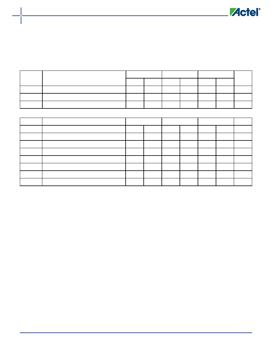
Table 26
Clock Specification for 33 MHz PCI
Symbol
Parameter
PCI
A42MX24
A42MX36
Units
Min.
Max.
Min.
Max.
Min.
Max.
tCYC
CLK Cycle Time
30
–
4.0
–
4.0
–
ns
tHIGH
CLK High Time
11
–
1.9
–
1.9
–
ns
tLOW
CLK Low Time
11
–1.9
–
ns
Table 27
Timing Parameters for 33 MHz PCI
PCI
A42MX24
A42MX36
Symbol
Parameter
Min.Max.Min.Max.Min.Max.
Units
tVAL
CLK to Signal Valid—Bused Signals
2
11
2.0
9.0
2.0
9.0
ns
tVAL(PTP)
CLK to Signal Valid—Point-to-Point
2 2
12
2.0
9.0
2.0
9.0
ns
tON
Float to Active
2
–
2.0
4.0
2.0
4.0
ns
tOFF
Active to Float
–
28
–
8.31
–8.31
ns
tSU
Input Set-Up Time to CLK—Bused Signals
7
–
1.5
–
1.5
–
ns
tSU(PTP)
Input Set-Up Time to CLK—Point-to-Point
10, 12 2
–1.5
–
1.5
–
ns
tH
Input Hold to CLK
0
–
0
–
0
–
ns
Notes:
1. TOFF is system dependent. MX PCI devices have 7.4 ns turn-off time, reflection is typically an additional 10 ns.
2. REQ# and GNT# are point-to-point signals and have different output valid delay and input setup times than do bussed signals.
GNT# has a setup of 10; REW# has a setup of 12.
相關PDF資料 |
PDF描述 |
|---|---|
| A40MX04-FPL84X79 | FPGA, 547 CLBS, 6000 GATES, 48 MHz, PQCC84 |
| A40MX04-FPL84 | FPGA, 547 CLBS, 6000 GATES, 48 MHz, PQCC84 |
| A40MX04-FPQ100X79 | FPGA, 547 CLBS, 6000 GATES, 48 MHz, PQFP100 |
| A40MX04-FPQ100 | FPGA, 547 CLBS, 6000 GATES, 48 MHz, PQFP100 |
| A40MX04-FVQ80X79 | FPGA, 547 CLBS, 6000 GATES, 48 MHz, PQFP80 |
相關代理商/技術參數 |
參數描述 |
|---|---|
| A40MX04-FPL68I | 制造商:未知廠家 制造商全稱:未知廠家 功能描述:Field Programmable Gate Array (FPGA) |
| A40MX04-FPL68M | 制造商:未知廠家 制造商全稱:未知廠家 功能描述:Field Programmable Gate Array (FPGA) |
| A40MX04-FPL84 | 功能描述:IC FPGA MX SGL CHIP 6K 84-PLCC RoHS:否 類別:集成電路 (IC) >> 嵌入式 - FPGA(現場可編程門陣列) 系列:MX 標準包裝:152 系列:IGLOO PLUS LAB/CLB數:- 邏輯元件/單元數:792 RAM 位總計:- 輸入/輸出數:120 門數:30000 電源電壓:1.14 V ~ 1.575 V 安裝類型:表面貼裝 工作溫度:-40°C ~ 85°C 封裝/外殼:289-TFBGA,CSBGA 供應商設備封裝:289-CSP(14x14) |
| A40MX04-FPL84I | 制造商:未知廠家 制造商全稱:未知廠家 功能描述:Field Programmable Gate Array (FPGA) |
| A40MX04-FPL84M | 制造商:未知廠家 制造商全稱:未知廠家 功能描述:Field Programmable Gate Array (FPGA) |
發布緊急采購,3分鐘左右您將得到回復。