- 您現在的位置:買賣IC網 > PDF目錄164976 > A40MX04-FPL84 FPGA, 547 CLBS, 6000 GATES, 48 MHz, PQCC84 PDF資料下載
參數資料
| 型號: | A40MX04-FPL84 |
| 元件分類: | FPGA |
| 英文描述: | FPGA, 547 CLBS, 6000 GATES, 48 MHz, PQCC84 |
| 封裝: | PLASTIC, LCC-84 |
| 文件頁數: | 1/124頁 |
| 文件大小: | 3142K |
| 代理商: | A40MX04-FPL84 |
當前第1頁第2頁第3頁第4頁第5頁第6頁第7頁第8頁第9頁第10頁第11頁第12頁第13頁第14頁第15頁第16頁第17頁第18頁第19頁第20頁第21頁第22頁第23頁第24頁第25頁第26頁第27頁第28頁第29頁第30頁第31頁第32頁第33頁第34頁第35頁第36頁第37頁第38頁第39頁第40頁第41頁第42頁第43頁第44頁第45頁第46頁第47頁第48頁第49頁第50頁第51頁第52頁第53頁第54頁第55頁第56頁第57頁第58頁第59頁第60頁第61頁第62頁第63頁第64頁第65頁第66頁第67頁第68頁第69頁第70頁第71頁第72頁第73頁第74頁第75頁第76頁第77頁第78頁第79頁第80頁第81頁第82頁第83頁第84頁第85頁第86頁第87頁第88頁第89頁第90頁第91頁第92頁第93頁第94頁第95頁第96頁第97頁第98頁第99頁第100頁第101頁第102頁第103頁第104頁第105頁第106頁第107頁第108頁第109頁第110頁第111頁第112頁第113頁第114頁第115頁第116頁第117頁第118頁第119頁第120頁第121頁第122頁第123頁第124頁
April 2009
i
2009 Actel Corporation
See the Actel website for the latest version of the datasheet.
v6.1
40MX and 42MX FPGA Families
Features
High Capacity
Single-Chip ASIC Alternative
3,000 to 54,000 System Gates
Up to 2.5 kbits Configurable Dual-Port SRAM
Fast Wide-Decode Circuitry
Up to 202 User-Programmable I/O Pins
High Performance
5.6 ns Clock-to-Out
250 MHz Performance
5 ns Dual-Port SRAM Access
100 MHz FIFOs
7.5 ns 35-Bit Address Decode
HiRel Features
Commercial, Industrial, Automotive, and Military
Temperature Plastic Packages
Commercial, Military Temperature, and MIL-STD-883
Ceramic Packages
QML Certification
Ceramic Devices Available to DSCC SMD
Ease of Integration
Mixed-Voltage Operation (5.0V or 3.3V for core and
I/Os), with PCI-Compliant I/Os
Up to 100% Resource Utilization and 100% Pin
Locking
Deterministic, User-Controllable Timing
Unique
In-System
Diagnostic
and
Verification
Capability with Silicon Explorer II
Low Power Consumption
IEEE Standard 1149.1 (JTAG) Boundary Scan Testing
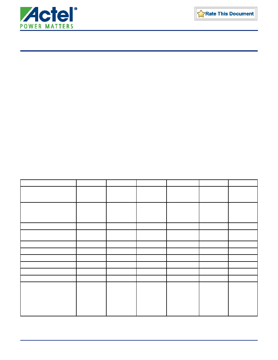
Product Profile
Device
A40MX02
A40MX04
A42MX09
A42MX16
A42MX24
A42MX36
Capacity
System Gates
SRAM Bits
3,000
–
6,000
–
14,000
–
24,000
–
36,000
–
54,000
2,560
Logic Modules
Sequential
Combinatorial
Decode
–
295
–
547
–
348
336
–
624
608
–
954
912
24
1,230
1,184
24
Clock-to-Out
9.5 ns
5.6 ns
6.1 ns
6.3 ns
SRAM Modules
(64x4 or 32x8)
–––
–
10
Dedicated Flip-Flops
–
348
624
954
1,230
Maximum Flip-Flops
147
273
516
928
1,410
1,822
Clocks
11
2
6
User I/O (maximum)
57
69
104
140
176
202
PCI
–––
–
Yes
Boundary Scan Test (BST)
–––
–
Yes
Packages (by pin count)
PLCC
PQFP
VQFP
TQFP
CQFP
PBGA
44, 68
100
80
–
44, 68, 84
100
80
–
84
100, 160
100
176
–
84
100, 160, 208
100
176
–
84
160, 208
–
176
–
208, 240
–
208, 256
272
相關PDF資料 |
PDF描述 |
|---|---|
| A40MX04-FPQ100X79 | FPGA, 547 CLBS, 6000 GATES, 48 MHz, PQFP100 |
| A40MX04-FPQ100 | FPGA, 547 CLBS, 6000 GATES, 48 MHz, PQFP100 |
| A40MX04-FVQ80X79 | FPGA, 547 CLBS, 6000 GATES, 48 MHz, PQFP80 |
| A40MX04-FVQ80 | FPGA, 547 CLBS, 6000 GATES, 48 MHz, PQFP80 |
| A40MX04-PL44IX79 | FPGA, 547 CLBS, 6000 GATES, 80 MHz, PQCC44 |
相關代理商/技術參數 |
參數描述 |
|---|---|
| A40MX04-FPL84I | 制造商:未知廠家 制造商全稱:未知廠家 功能描述:Field Programmable Gate Array (FPGA) |
| A40MX04-FPL84M | 制造商:未知廠家 制造商全稱:未知廠家 功能描述:Field Programmable Gate Array (FPGA) |
| A40MX04-FPLG44 | 功能描述:IC FPGA MX SGL CHIP 6K 44-PLCC RoHS:是 類別:集成電路 (IC) >> 嵌入式 - FPGA(現場可編程門陣列) 系列:MX 標準包裝:152 系列:IGLOO PLUS LAB/CLB數:- 邏輯元件/單元數:792 RAM 位總計:- 輸入/輸出數:120 門數:30000 電源電壓:1.14 V ~ 1.575 V 安裝類型:表面貼裝 工作溫度:-40°C ~ 85°C 封裝/外殼:289-TFBGA,CSBGA 供應商設備封裝:289-CSP(14x14) |
| A40MX04-FPLG68 | 功能描述:IC FPGA MX SGL CHIP 6K 68-PLCC RoHS:是 類別:集成電路 (IC) >> 嵌入式 - FPGA(現場可編程門陣列) 系列:MX 標準包裝:152 系列:IGLOO PLUS LAB/CLB數:- 邏輯元件/單元數:792 RAM 位總計:- 輸入/輸出數:120 門數:30000 電源電壓:1.14 V ~ 1.575 V 安裝類型:表面貼裝 工作溫度:-40°C ~ 85°C 封裝/外殼:289-TFBGA,CSBGA 供應商設備封裝:289-CSP(14x14) |
| A40MX04-FPLG84 | 功能描述:IC FPGA MX SGL CHIP 6K 84-PLCC RoHS:是 類別:集成電路 (IC) >> 嵌入式 - FPGA(現場可編程門陣列) 系列:MX 標準包裝:152 系列:IGLOO PLUS LAB/CLB數:- 邏輯元件/單元數:792 RAM 位總計:- 輸入/輸出數:120 門數:30000 電源電壓:1.14 V ~ 1.575 V 安裝類型:表面貼裝 工作溫度:-40°C ~ 85°C 封裝/外殼:289-TFBGA,CSBGA 供應商設備封裝:289-CSP(14x14) |
發布緊急采購,3分鐘左右您將得到回復。