- 您現在的位置:買賣IC網 > PDF目錄164976 > A40MX04-FPL84 FPGA, 547 CLBS, 6000 GATES, 48 MHz, PQCC84 PDF資料下載
參數資料
| 型號: | A40MX04-FPL84 |
| 元件分類: | FPGA |
| 英文描述: | FPGA, 547 CLBS, 6000 GATES, 48 MHz, PQCC84 |
| 封裝: | PLASTIC, LCC-84 |
| 文件頁數: | 32/124頁 |
| 文件大小: | 3142K |
| 代理商: | A40MX04-FPL84 |
第1頁第2頁第3頁第4頁第5頁第6頁第7頁第8頁第9頁第10頁第11頁第12頁第13頁第14頁第15頁第16頁第17頁第18頁第19頁第20頁第21頁第22頁第23頁第24頁第25頁第26頁第27頁第28頁第29頁第30頁第31頁當前第32頁第33頁第34頁第35頁第36頁第37頁第38頁第39頁第40頁第41頁第42頁第43頁第44頁第45頁第46頁第47頁第48頁第49頁第50頁第51頁第52頁第53頁第54頁第55頁第56頁第57頁第58頁第59頁第60頁第61頁第62頁第63頁第64頁第65頁第66頁第67頁第68頁第69頁第70頁第71頁第72頁第73頁第74頁第75頁第76頁第77頁第78頁第79頁第80頁第81頁第82頁第83頁第84頁第85頁第86頁第87頁第88頁第89頁第90頁第91頁第92頁第93頁第94頁第95頁第96頁第97頁第98頁第99頁第100頁第101頁第102頁第103頁第104頁第105頁第106頁第107頁第108頁第109頁第110頁第111頁第112頁第113頁第114頁第115頁第116頁第117頁第118頁第119頁第120頁第121頁第122頁第123頁第124頁
40MX and 42MX FPGA Families
v6.1
1-9
Fixed Capacitance Values for MX FPGAs (pF)
Test Circuitry and Silicon Explorer II Probe
MX devices contain probing circuitry that provides built-
in access to every node in a design, via the use of Silicon
Explorer II. Silicon Explorer II is an integrated hardware
and software solution that, in conjunction with the
Designer software, allow users to examine any of the
internal nets of the device while it is operating in a
prototyping or a production system. The user can probe
into an MX device without changing the placement and
routing of the design and without using any additional
resources. Silicon Explorer II's noninvasive method does
not alter timing or loading effects, thus shortening the
debug cycle and providing a true representation of the
device under actual functional situations.
Silicon
Explorer
II
samples
data
at
100
MHz
(asynchronous) or 66 MHz (synchronous). Silicon Explorer
II attaches to a PC's standard COM port, turning the PC
into a fully functional 18-channel logic analyzer. Silicon
Explorer II allows designers to complete the design
verification
process
at
their
desks
and
reduces
verification time from several hours per cycle to a few
seconds.
Silicon Explorer II is used to control the MODE, DCLK, SDI
and SDO pins in MX devices to select the desired nets for
debugging. The user simply assigns the selected internal
nets in the Silicon Explorer II software to the PRA/PRB
output pins for observation. Probing functionality is
activated when the MODE pin is held HIGH.
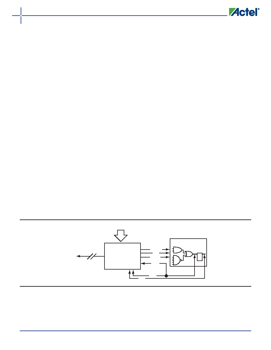
Figure 1-12 illustrates the interconnection between
Silicon Explorer II and 40MX devices, while Figure 1-13
on page 1-10 illustrates the interconnection between
Silicon Explorer II and 42MX devices
To allow for probing capabilities, the security fuses must
not be programmed. (Refer to <zBlue>“User Security”
section on page 6 for the security fuses of 40MX and
42MX devices). Table 2 on page 1-10 summarizes the
possible device configurations for probing.
PRA and PRB pins are dual-purpose pins. When the
"Reserve
Probe
Pin"
is
checked
in
the
Designer software, PRA and PRB pins are reserved as
dedicated outputs for probing. If PRA and PRB pins are
required as user I/Os to achieve successful layout and
"Reserve Probe Pin" is checked, the layout tool will
override the option and place user I/Os on PRA and PRB
pins.
CEQM = Equivalent capacitance of logic modules in pF
CEQI = Equivalent capacitance of input buffers in pF
CEQO = Equivalent capacitance of output buffers in pF
CEQCR = Equivalent capacitance of routed array clock in
pF
CL
= Output load capacitance in pF
fm
= Average logic module switching rate in MHz
fn
= Average input buffer switching rate in MHz
fp
= Average output buffer switching rate in MHz
fq1
= Average first routed array clock rate in MHz
fq2
= Average second routed array clock rate in MHz
Device Type
r1
routed_Clk1
r2
routed_Clk2
A40MX02
41.4
N/A
A40MX04
68.6
N/A
A42MX09
118
A42MX16
165
A42MX24
185
A42MX36
220
Figure 1-12 Silicon Explorer II Setup with 40MX
40MX
Silicon
Explorer II
PRA
PRB
SDO
DCLK
SDI
MODE
Serial Connection
to Windows PC
16 Logic Analyzer Channels
相關PDF資料 |
PDF描述 |
|---|---|
| A40MX04-FPQ100X79 | FPGA, 547 CLBS, 6000 GATES, 48 MHz, PQFP100 |
| A40MX04-FPQ100 | FPGA, 547 CLBS, 6000 GATES, 48 MHz, PQFP100 |
| A40MX04-FVQ80X79 | FPGA, 547 CLBS, 6000 GATES, 48 MHz, PQFP80 |
| A40MX04-FVQ80 | FPGA, 547 CLBS, 6000 GATES, 48 MHz, PQFP80 |
| A40MX04-PL44IX79 | FPGA, 547 CLBS, 6000 GATES, 80 MHz, PQCC44 |
相關代理商/技術參數 |
參數描述 |
|---|---|
| A40MX04-FPL84I | 制造商:未知廠家 制造商全稱:未知廠家 功能描述:Field Programmable Gate Array (FPGA) |
| A40MX04-FPL84M | 制造商:未知廠家 制造商全稱:未知廠家 功能描述:Field Programmable Gate Array (FPGA) |
| A40MX04-FPLG44 | 功能描述:IC FPGA MX SGL CHIP 6K 44-PLCC RoHS:是 類別:集成電路 (IC) >> 嵌入式 - FPGA(現場可編程門陣列) 系列:MX 標準包裝:152 系列:IGLOO PLUS LAB/CLB數:- 邏輯元件/單元數:792 RAM 位總計:- 輸入/輸出數:120 門數:30000 電源電壓:1.14 V ~ 1.575 V 安裝類型:表面貼裝 工作溫度:-40°C ~ 85°C 封裝/外殼:289-TFBGA,CSBGA 供應商設備封裝:289-CSP(14x14) |
| A40MX04-FPLG68 | 功能描述:IC FPGA MX SGL CHIP 6K 68-PLCC RoHS:是 類別:集成電路 (IC) >> 嵌入式 - FPGA(現場可編程門陣列) 系列:MX 標準包裝:152 系列:IGLOO PLUS LAB/CLB數:- 邏輯元件/單元數:792 RAM 位總計:- 輸入/輸出數:120 門數:30000 電源電壓:1.14 V ~ 1.575 V 安裝類型:表面貼裝 工作溫度:-40°C ~ 85°C 封裝/外殼:289-TFBGA,CSBGA 供應商設備封裝:289-CSP(14x14) |
| A40MX04-FPLG84 | 功能描述:IC FPGA MX SGL CHIP 6K 84-PLCC RoHS:是 類別:集成電路 (IC) >> 嵌入式 - FPGA(現場可編程門陣列) 系列:MX 標準包裝:152 系列:IGLOO PLUS LAB/CLB數:- 邏輯元件/單元數:792 RAM 位總計:- 輸入/輸出數:120 門數:30000 電源電壓:1.14 V ~ 1.575 V 安裝類型:表面貼裝 工作溫度:-40°C ~ 85°C 封裝/外殼:289-TFBGA,CSBGA 供應商設備封裝:289-CSP(14x14) |
發布緊急采購,3分鐘左右您將得到回復。