- 您現在的位置:買賣IC網 > PDF目錄164976 > A40MX04-FVQ80X79 FPGA, 547 CLBS, 6000 GATES, 48 MHz, PQFP80 PDF資料下載
參數資料
| 型號: | A40MX04-FVQ80X79 |
| 元件分類: | FPGA |
| 英文描述: | FPGA, 547 CLBS, 6000 GATES, 48 MHz, PQFP80 |
| 封裝: | 1 MM HEIGHT, PLASTIC, VQFP-80 |
| 文件頁數: | 34/124頁 |
| 文件大小: | 3142K |
| 代理商: | A40MX04-FVQ80X79 |
第1頁第2頁第3頁第4頁第5頁第6頁第7頁第8頁第9頁第10頁第11頁第12頁第13頁第14頁第15頁第16頁第17頁第18頁第19頁第20頁第21頁第22頁第23頁第24頁第25頁第26頁第27頁第28頁第29頁第30頁第31頁第32頁第33頁當前第34頁第35頁第36頁第37頁第38頁第39頁第40頁第41頁第42頁第43頁第44頁第45頁第46頁第47頁第48頁第49頁第50頁第51頁第52頁第53頁第54頁第55頁第56頁第57頁第58頁第59頁第60頁第61頁第62頁第63頁第64頁第65頁第66頁第67頁第68頁第69頁第70頁第71頁第72頁第73頁第74頁第75頁第76頁第77頁第78頁第79頁第80頁第81頁第82頁第83頁第84頁第85頁第86頁第87頁第88頁第89頁第90頁第91頁第92頁第93頁第94頁第95頁第96頁第97頁第98頁第99頁第100頁第101頁第102頁第103頁第104頁第105頁第106頁第107頁第108頁第109頁第110頁第111頁第112頁第113頁第114頁第115頁第116頁第117頁第118頁第119頁第120頁第121頁第122頁第123頁第124頁
40MX and 42MX FPGA Families
v6.1
1-11
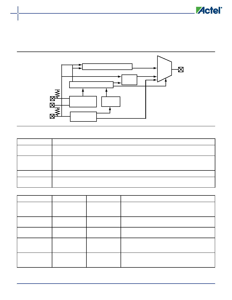
Each I/O cell has three boundary-scan register cells, each
with a serial-in, serial-out, parallel-in, and parallel-out
pin. The serial pins are used to serially connect all the
boundary-scan register cells in a device into a boundary-
scan register chain, which starts at the TDI pin and ends
at the TDO pin. The parallel ports are connected to the
internal core logic tile and the input, output and control
ports of an I/O buffer to capture and load data into the
register to control or observe the logic state of each I/O.
Figure 1-14 42MX IEEE 1149.1 Boundary Scan Circuitry
Table 3
Test Access Port Descriptions
Port
Description
TMS
(Test
Mode
Select)
Serial input for the test logic control bits. Data is captured on the rising edge of the test logic clock (TCK).
TCK (Test Clock Input) Dedicated test logic clock used serially to shift test instruction, test data, and control inputs on the rising edge
of the clock, and serially to shift the output data on the falling edge of the clock. The maximum clock frequency
for TCK is 20 MHz.
TDI (Test Data Input)
Serial input for instruction and test data. Data is captured on the rising edge of the test logic clock.
TDO
(Test
Data
Output)
Serial output for test instruction and data from the test logic. TDO is set to an Inactive Drive state (high
impedance) when data scanning is not in progress.
Table 4
Supported BST Public Instructions
Instruction
IR Code (IR2.IR0)
Instruction Type
Description
EXTEST
000
Mandatory
Allows the external circuitry and board-level interconnections to
be tested by forcing a test pattern at the output pins and
capturing test results at the input pins.
SAMPLE/PRELOAD
001
Mandatory
Allows a snapshot of the signals at the device pins to be
captured and examined during operation
HIGH Z
101
Optional
Tristates all I/Os to allow external signals to drive pins. Please
refer to the IEEE Standard 1149.1 specification.
CLAMP
110
Optional
Allows state of signals driven from component pins to be
determined from the Boundary-Scan Register. Please refer to
the IEEE Standard 1149.1 specification for details.
BYPASS
111
Mandatory
Enables the bypass register between the TDI and TDO pins. The
test data passes through the selected device to adjacent devices
in the test chain.
Boundary Scan Register
Instruction
Decode
Control Logic
TAP Controller
Instruction
Register
Bypass
Register
TMS
TCK
TDI
Output
MUX
TDO
JTAG
相關PDF資料 |
PDF描述 |
|---|---|
| A40MX04-FVQ80 | FPGA, 547 CLBS, 6000 GATES, 48 MHz, PQFP80 |
| A40MX04-PL44IX79 | FPGA, 547 CLBS, 6000 GATES, 80 MHz, PQCC44 |
| A40MX04-PL44I | FPGA, 547 CLBS, 6000 GATES, 80 MHz, PQCC44 |
| A40MX04-PL44MX79 | FPGA, 547 CLBS, 6000 GATES, 80 MHz, PQCC44 |
| A40MX04-PL44M | FPGA, 547 CLBS, 6000 GATES, 80 MHz, PQCC44 |
相關代理商/技術參數 |
參數描述 |
|---|---|
| A40MX04-FVQG80 | 功能描述:IC FPGA MX SGL CHIP 6K 80-VQFP RoHS:是 類別:集成電路 (IC) >> 嵌入式 - FPGA(現場可編程門陣列) 系列:MX 標準包裝:152 系列:IGLOO PLUS LAB/CLB數:- 邏輯元件/單元數:792 RAM 位總計:- 輸入/輸出數:120 門數:30000 電源電壓:1.14 V ~ 1.575 V 安裝類型:表面貼裝 工作溫度:-40°C ~ 85°C 封裝/外殼:289-TFBGA,CSBGA 供應商設備封裝:289-CSP(14x14) |
| A40MX04-PL100 | 制造商:ACTEL 制造商全稱:Actel Corporation 功能描述:40MX and 42MX FPGA Families |
| A40MX04-PL100ES | 制造商:ACTEL 制造商全稱:Actel Corporation 功能描述:40MX and 42MX FPGA Families |
| A40MX04-PL100I | 制造商:ACTEL 制造商全稱:Actel Corporation 功能描述:40MX and 42MX FPGA Families |
| A40MX04-PL100M | 制造商:ACTEL 制造商全稱:Actel Corporation 功能描述:40MX and 42MX FPGA Families |
發布緊急采購,3分鐘左右您將得到回復。