- 您現在的位置:買賣IC網 > PDF目錄164976 > A40MX04-FVQ80X79 FPGA, 547 CLBS, 6000 GATES, 48 MHz, PQFP80 PDF資料下載
參數資料
| 型號: | A40MX04-FVQ80X79 |
| 元件分類: | FPGA |
| 英文描述: | FPGA, 547 CLBS, 6000 GATES, 48 MHz, PQFP80 |
| 封裝: | 1 MM HEIGHT, PLASTIC, VQFP-80 |
| 文件頁數: | 62/124頁 |
| 文件大小: | 3142K |
| 代理商: | A40MX04-FVQ80X79 |
第1頁第2頁第3頁第4頁第5頁第6頁第7頁第8頁第9頁第10頁第11頁第12頁第13頁第14頁第15頁第16頁第17頁第18頁第19頁第20頁第21頁第22頁第23頁第24頁第25頁第26頁第27頁第28頁第29頁第30頁第31頁第32頁第33頁第34頁第35頁第36頁第37頁第38頁第39頁第40頁第41頁第42頁第43頁第44頁第45頁第46頁第47頁第48頁第49頁第50頁第51頁第52頁第53頁第54頁第55頁第56頁第57頁第58頁第59頁第60頁第61頁當前第62頁第63頁第64頁第65頁第66頁第67頁第68頁第69頁第70頁第71頁第72頁第73頁第74頁第75頁第76頁第77頁第78頁第79頁第80頁第81頁第82頁第83頁第84頁第85頁第86頁第87頁第88頁第89頁第90頁第91頁第92頁第93頁第94頁第95頁第96頁第97頁第98頁第99頁第100頁第101頁第102頁第103頁第104頁第105頁第106頁第107頁第108頁第109頁第110頁第111頁第112頁第113頁第114頁第115頁第116頁第117頁第118頁第119頁第120頁第121頁第122頁第123頁第124頁
40MX and 42MX FPGA Families
1- 36
v6.1
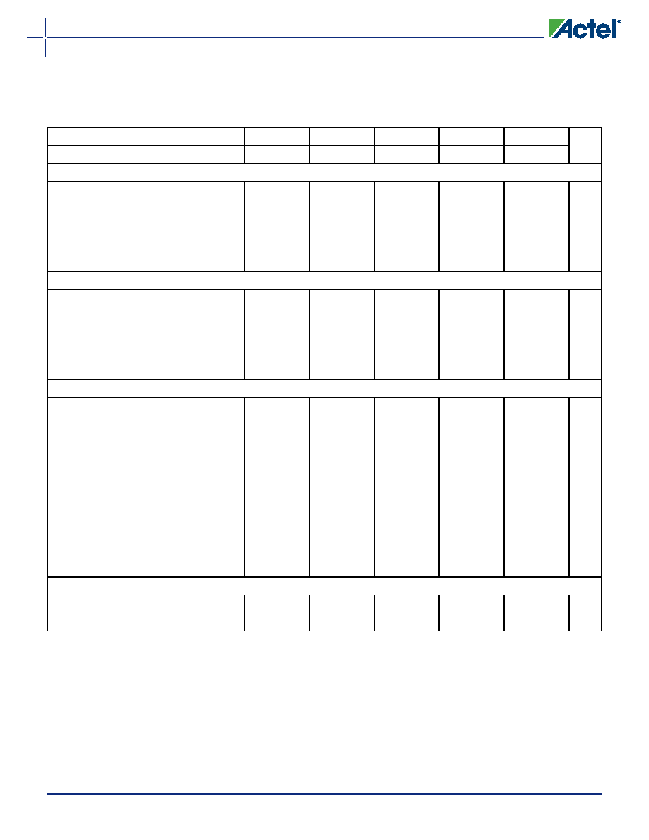
Timing Characteristics
Table 28
A40MX02 Timing Characteristics (Nominal 5.0V Operation)
(Worst-Case Commercial Conditions, VCC = 4.75V, TJ = 70°C)
‘–3’ Speed
‘–2’ Speed
‘–1’ Speed
‘Std’ Speed
‘–F’ Speed
Units
Parameter Description
Min.
Max.
Min.
Max.
Min.
Max.
Min.
Max.
Min.
Max.
Logic Module Propagation Delays
tPD1
Single Module
1.2
1.4
1.6
1.9
2.7
ns
tPD2
Dual-Module Macros
2.7
3.1
3.5
4.1
5.7
ns
tCO
Sequential Clock-to-Q
1.2
1.4
1.6
1.9
2.7
ns
tGO
Latch G-to-Q
1.2
1.4
1.6
1.9
2.7
ns
tRS
Flip-Flop (Latch) Reset-to-Q
1.2
1.4
1.6
1.9
2.7
ns
Logic Module Predicted Routing Delays1
tRD1
FO=1 Routing Delay
1.3
1.5
1.7
2.0
2.8
ns
tRD2
FO=2 Routing Delay
1.8
2.1
2.4
2.8
3.9
ns
tRD3
FO=3 Routing Delay
2.3
2.7
3.0
3.6
5.0
ns
tRD4
FO=4 Routing Delay
2.9
3.3
3.7
4.4
6.1
ns
tRD8
FO=8 Routing Delay
4.9
5.7
6.5
7.6
10.6
ns
Logic Module Sequential Timing2
tSUD
Flip-Flop (Latch) Data Input Set-Up
3.1
3.5
4.0
4.7
6.6
ns
tHD
3
Flip-Flop (Latch) Data Input Hold
0.0
ns
tSUENA
Flip-Flop (Latch) Enable Set-Up
3.1
3.5
4.0
4.7
6.6
ns
tHENA
Flip-Flop (Latch) Enable Hold
0.0
ns
tWCLKA
Flip-Flop (Latch)
Clock Active Pulse Width
3.3
3.8
4.3
5.0
7.0
ns
tWASYN
Flip-Flop (Latch)
Asynchronous Pulse Width
3.3
3.8
4.3
5.0
7.0
ns
tA
Flip-Flop Clock Input Period
4.8
5.6
6.3
7.5
10.4
ns
fMAX
Flip-Flop (Latch) Clock
Frequency (FO = 128)
181
168
154
134
80
MHz
Input Module Propagation Delays
tINYH
Pad-to-Y HIGH
0.7
0.8
0.9
1.1
1.5
ns
tINYL
Pad-to-Y LOW
0.6
0.7
0.8
1.0
1.3
ns
Notes:
1. Routing delays are for typical designs across worst-case operating conditions. These parameters should be used for estimating
device performance. Post-route timing analysis or simulation is required to determine actual performance.
2. Set-up times assume fanout of 3. Further testing information can be obtained from the Timer utility.
3. The hold time for the DFME1A macro may be greater than 0 ns. Use the Timer tool from the Designer software to check the hold
time for this macro.
4. Delays based on 35pF loading.
相關PDF資料 |
PDF描述 |
|---|---|
| A40MX04-FVQ80 | FPGA, 547 CLBS, 6000 GATES, 48 MHz, PQFP80 |
| A40MX04-PL44IX79 | FPGA, 547 CLBS, 6000 GATES, 80 MHz, PQCC44 |
| A40MX04-PL44I | FPGA, 547 CLBS, 6000 GATES, 80 MHz, PQCC44 |
| A40MX04-PL44MX79 | FPGA, 547 CLBS, 6000 GATES, 80 MHz, PQCC44 |
| A40MX04-PL44M | FPGA, 547 CLBS, 6000 GATES, 80 MHz, PQCC44 |
相關代理商/技術參數 |
參數描述 |
|---|---|
| A40MX04-FVQG80 | 功能描述:IC FPGA MX SGL CHIP 6K 80-VQFP RoHS:是 類別:集成電路 (IC) >> 嵌入式 - FPGA(現場可編程門陣列) 系列:MX 標準包裝:152 系列:IGLOO PLUS LAB/CLB數:- 邏輯元件/單元數:792 RAM 位總計:- 輸入/輸出數:120 門數:30000 電源電壓:1.14 V ~ 1.575 V 安裝類型:表面貼裝 工作溫度:-40°C ~ 85°C 封裝/外殼:289-TFBGA,CSBGA 供應商設備封裝:289-CSP(14x14) |
| A40MX04-PL100 | 制造商:ACTEL 制造商全稱:Actel Corporation 功能描述:40MX and 42MX FPGA Families |
| A40MX04-PL100ES | 制造商:ACTEL 制造商全稱:Actel Corporation 功能描述:40MX and 42MX FPGA Families |
| A40MX04-PL100I | 制造商:ACTEL 制造商全稱:Actel Corporation 功能描述:40MX and 42MX FPGA Families |
| A40MX04-PL100M | 制造商:ACTEL 制造商全稱:Actel Corporation 功能描述:40MX and 42MX FPGA Families |
發布緊急采購,3分鐘左右您將得到回復。