- 您現在的位置:買賣IC網 > PDF目錄373912 > AD7665 (Analog Devices, Inc.) TV 8C 8#20 PIN PLUG PDF資料下載
參數資料
| 型號: | AD7665 |
| 廠商: | Analog Devices, Inc. |
| 英文描述: | TV 8C 8#20 PIN PLUG |
| 中文描述: | 16位,570 kSPS的的CMOS模數轉換器 |
| 文件頁數: | 14/24頁 |
| 文件大小: | 348K |
| 代理商: | AD7665 |
REV. 0
AD7665
–14–
TYPICAL CONNECTION DIAGRAM
Figure 5 shows a typical connection diagram for the AD7665.
Different circuitry shown on this diagram is optional and is
discussed below.
Analog Inputs
The AD7665 is specified to operate with six full-scale analog
input ranges. Connections required for each of the four ana-
log inputs, IND, INC, INB, INA, and the resulting full-scale
ranges, are shown in Table I. The typical input impedance
for each analog input range is also shown.
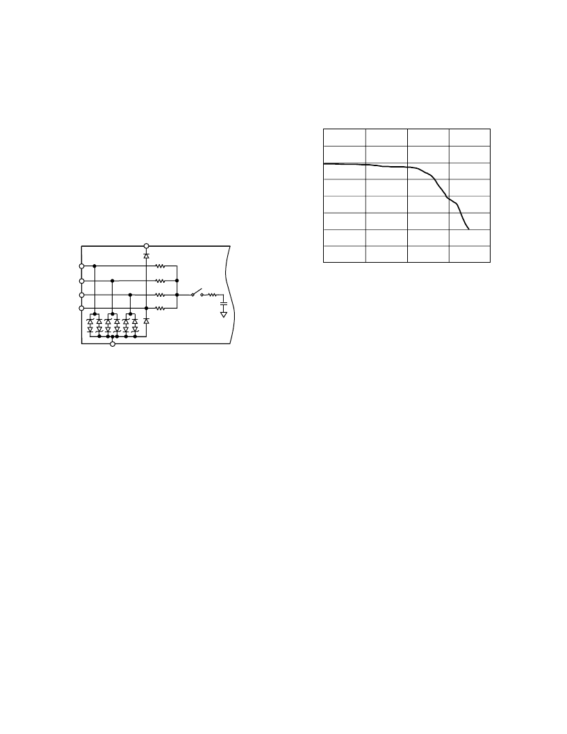
Figure 6 shows a simplified analog input section of the AD7665.
The four resistors connected to the four analog inputs form a
resistive scaler which scales-down and shifts the analog input
range to a common input range of 0 V to 2.5 V at the input of
the switched capacitive ADC.
INC
INB
INA
4R
2R
R
IND
4R
AGND
AVDD
R1
C
S
R = 1.28k
Figure 6. Simplified Analog Input
By connecting the four inputs INA, INB, INC, IND to the input
signal itself, the ground, or a 2.5 V reference, other analog input
ranges can be obtained.
The diodes shown in Figure 6 provide ESD protection for the
four analog inputs. The inputs INB, INC, IND, have a high
voltage protection (–11 V to +30 V) to allow wide input voltage
range. Care must be taken to ensure that the analog input signal
never exceeds the absolute ratings on these inputs including
INA (0 V to 5 V). This will cause these diodes to become forward-
biased and start conducting current. These diodes can handle a
forward-biased current of 120 mA maximum. For instance, when
using the 0 V to 2.5 V input range, these conditions could eventu-
ally occur on the input INA when the input buffer’s (U1) supplies
are different from AVDD. In such case, an input buffer with a
short-circuit current limitation can be used to protect the part.
This analog input structure allows the sampling of the differen-
tial signal between the output of the resistive scaler and INGND.
Unlike other converters, the INGND input is sampled at the
same time as the inputs. By using this differential input, small
signals common to both inputs are rejected as shown in Figure 7,
which represents the typical CMRR over frequency. For instance,
by using INGND to sense a remote signal ground, difference of
ground potentials between the sensor and the local ADC ground
are eliminated.
75
70
65
60
55
50
45
40
35
1 10 100 1000 10000
FREQUENCY
–
kHz
C
–
Figure 7. Analog Input CMRR vs. Frequency
During the acquisition phase for ac signals, the AD7665 behaves
like a one-pole RC filter consisting of the equivalent resistance
of the resistive scaler R/2 in series with R1 and C
S
. The resistor
R1 is typically 100
and is a lumped component made up of
some serial resistor and the on-resistance of the switches.
The capacitor C
S
is typically 60 pF and is mainly the ADC
sampling capacitor. This one-pole filter with a typical –3 dB
cutoff frequency of 3.6 MHz reduces undesirable aliasing effects
and limits the noise coming from the inputs.
Except when using the 0 V to 2.5 V analog input voltage range,
the AD7665 has to be driven by a very low impedance source to
avoid gain errors. That can be done by using a driver amplifier
whose choice is eased by the primarily resistive analog input
circuitry of the AD7665.
When using the 0 V to 2.5 V analog input voltage range, the
input impedance of the AD7665 is very high so the AD7665 can
be driven directly by a low impedance source without gain error.
That allows, as shown in Figure 5, putting an external one-
pole RC filter between the output of the amplifier output and
the ADC analog inputs to even further improve the noise
filtering done by the AD7665 analog input circuit. However, the
source impedance has to be kept low because it affects the ac
performances, especially the total harmonic distortion (THD).
The maximum source impedance depends on the amount of
total THD that can be tolerated. The THD degradation is a
function of the source impedance and the maximum input
frequency as shown in Figure 8.
相關PDF資料 |
PDF描述 |
|---|---|
| AD7665AST | 16-Bit, 570 kSPS CMOS ADC |
| AD7665ASTRL | 16-Bit, 570 kSPS CMOS ADC |
| AD7669AN | LC2MOS Complete, 8-Bit Analog I/0 Systems |
| AD7569TE | LC2MOS Complete, 8-Bit Analog I/0 Systems |
| AD7569KN | LC2MOS Complete, 8-Bit Analog I/0 Systems |
相關代理商/技術參數 |
參數描述 |
|---|---|
| AD7665ACP | 制造商:Analog Devices 功能描述:ADC Single SAR 570ksps 16-bit Parallel/Serial 48-Pin LFCSP EP 制造商:Rochester Electronics LLC 功能描述:16-BIT, 500 KSPS CMOS A/D CONVERTER - Bulk |
| AD7665ACPRL | 制造商:Analog Devices 功能描述:ADC Single SAR 570ksps 16-bit Parallel/Serial 48-Pin LFCSP EP T/R |
| AD7665ACPZ | 功能描述:IC ADC 16BIT CMOS 5V 48LFCSP RoHS:是 類別:集成電路 (IC) >> 數據采集 - 模數轉換器 系列:PulSAR® 標準包裝:1 系列:- 位數:14 采樣率(每秒):83k 數據接口:串行,并聯 轉換器數目:1 功率耗散(最大):95mW 電壓電源:雙 ± 工作溫度:0°C ~ 70°C 安裝類型:通孔 封裝/外殼:28-DIP(0.600",15.24mm) 供應商設備封裝:28-PDIP 包裝:管件 輸入數目和類型:1 個單端,雙極 |
| AD7665ACPZRL | 功能描述:IC ADC 16BIT CMOS 5V 48LFCSP RoHS:是 類別:集成電路 (IC) >> 數據采集 - 模數轉換器 系列:PulSAR® 標準包裝:1 系列:- 位數:14 采樣率(每秒):83k 數據接口:串行,并聯 轉換器數目:1 功率耗散(最大):95mW 電壓電源:雙 ± 工作溫度:0°C ~ 70°C 安裝類型:通孔 封裝/外殼:28-DIP(0.600",15.24mm) 供應商設備封裝:28-PDIP 包裝:管件 輸入數目和類型:1 個單端,雙極 |
| AD7665AST | 制造商:Rochester Electronics LLC 功能描述: 制造商:Analog Devices 功能描述:Analog-Digital Converter IC Number of Bi |
發布緊急采購,3分鐘左右您將得到回復。