- 您現在的位置:買賣IC網 > PDF目錄373912 > AD7665 (Analog Devices, Inc.) TV 8C 8#20 PIN PLUG PDF資料下載
參數資料
| 型號: | AD7665 |
| 廠商: | Analog Devices, Inc. |
| 英文描述: | TV 8C 8#20 PIN PLUG |
| 中文描述: | 16位,570 kSPS的的CMOS模數轉換器 |
| 文件頁數: | 19/24頁 |
| 文件大小: | 348K |
| 代理商: | AD7665 |
REV. 0
AD7665
–19–
CS
SCLK
SDOUT
D15
D14
D1
D0
D13
X15
X14
X13
X1
X0
Y15
Y14
BUSY
SDIN
INVSCLK = 0
t
35
t
36
t
37
t
31
t
32
t
16
t
33
t
34
X15
X14
X
1
2
3
14
15
16
17
18
EXT/
INT
= 1
RD
= 0
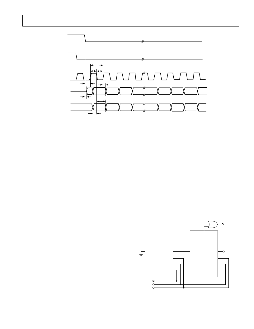
Figure 19. Slave Serial Data Timing for Reading (Read After Convert)
In read-during-conversion mode, the serial clock and data toggle
at appropriate instants which minimizes potential feedthrough
between digital activity and the critical conversion decisions.
In read-after-conversion mode, it should be noted that, unlike in
other modes, the signal BUSY returns low after the 16 data bits
are pulsed out and not at the end of the conversion phase which
results in a longer BUSY width.
SLAVE SERIAL INTERFACE
External Clock
The AD7665 is configured to accept an externally supplied
serial data clock on the SCLK pin when the EXT/
INT
pin is
held high. In this mode, several methods can be used to read the
data. The external serial clock is gated by
CS
and the data are
output when both
CS
and
RD
are low. Thus, depending on
CS
,
the data can be read after each conversion or during the follow-
ing conversion. The external clock can be either a continuous or
discontinuous clock. A discontinuous clock can be either nor-
mally high or normally low when inactive. Figure 19 and Figure
21 show the detailed timing diagrams of these methods.
While the AD7665 is performing a bit decision, it is important
that voltage transients not occur on digital input/output pins or
degradation of the conversion result could occur. This is par-
ticularly important during the second half of the conversion
phase because the AD7665 provides error correction circuitry
that can correct for an improper bit decision made during the
first half of the conversion phase. For this reason, it is recom-
mended that when an external clock is being provided, it is a
discontinuous clock that is toggling only when BUSY is low or,
more importantly, that is does not transition during the latter
half of BUSY high.
External Discontinuous Clock Data Read After Conversion
Though the maximum throughput cannot be achieved using this
mode, it is the most recommended of the serial slave modes.
Figure 19 shows the detailed timing diagrams of this method.
After a conversion is complete, indicated by BUSY returning
low, the result of this conversion can be read while both
CS
and
RD
are low. The data is shifted out, MSB first, with 16 clock
pulses and is valid on both rising and falling edge of the clock.
Among the advantages of this method, the conversion perfor-
mance is not degraded because there are no voltage transients on
the digital interface during the conversion process.
Another advantage is to be able to read the data at any speed up
to 40 MHz which accommodates both slow digital host interface
and the fastest serial reading.
Finally, in this mode only, the AD7665 provides a “daisy chain”
feature using the RDC/SDIN input pin for cascading multiple
converters together. This feature is useful for reducing compo-
nent count and wiring connections when desired as, for instance,
in isolated multiconverter applications.
An example of the concatenation of two devices is shown in Fig-
ure 20. Simultaneous sampling is possible by using a common
CNVST
signal. It should be noted that the RDC/SDIN input is
latched on the opposite edge of SCLK of the one used to shift out
the data on SDOUT. Hence, the MSB of the “upstream” con-
verter just follows the LSB of the “downstream” converter on
the next SCLK cycle.
CNVST
CS
SCLK
SDOUT
RDC/SDIN
BUSY
BUSY
DATA
OUT
AD7665
#1
(DOWNSTREAM)
BUSY
OUT
CNVST
CS
SCLK
AD7665
#2
(UPSTREAM)
RDC/SDIN
SDOUT
SCLK IN
CS IN
CNVST IN
Figure 20. Two AD7665s in a Daisy-Chain Configuration
相關PDF資料 |
PDF描述 |
|---|---|
| AD7665AST | 16-Bit, 570 kSPS CMOS ADC |
| AD7665ASTRL | 16-Bit, 570 kSPS CMOS ADC |
| AD7669AN | LC2MOS Complete, 8-Bit Analog I/0 Systems |
| AD7569TE | LC2MOS Complete, 8-Bit Analog I/0 Systems |
| AD7569KN | LC2MOS Complete, 8-Bit Analog I/0 Systems |
相關代理商/技術參數 |
參數描述 |
|---|---|
| AD7665ACP | 制造商:Analog Devices 功能描述:ADC Single SAR 570ksps 16-bit Parallel/Serial 48-Pin LFCSP EP 制造商:Rochester Electronics LLC 功能描述:16-BIT, 500 KSPS CMOS A/D CONVERTER - Bulk |
| AD7665ACPRL | 制造商:Analog Devices 功能描述:ADC Single SAR 570ksps 16-bit Parallel/Serial 48-Pin LFCSP EP T/R |
| AD7665ACPZ | 功能描述:IC ADC 16BIT CMOS 5V 48LFCSP RoHS:是 類別:集成電路 (IC) >> 數據采集 - 模數轉換器 系列:PulSAR® 標準包裝:1 系列:- 位數:14 采樣率(每秒):83k 數據接口:串行,并聯 轉換器數目:1 功率耗散(最大):95mW 電壓電源:雙 ± 工作溫度:0°C ~ 70°C 安裝類型:通孔 封裝/外殼:28-DIP(0.600",15.24mm) 供應商設備封裝:28-PDIP 包裝:管件 輸入數目和類型:1 個單端,雙極 |
| AD7665ACPZRL | 功能描述:IC ADC 16BIT CMOS 5V 48LFCSP RoHS:是 類別:集成電路 (IC) >> 數據采集 - 模數轉換器 系列:PulSAR® 標準包裝:1 系列:- 位數:14 采樣率(每秒):83k 數據接口:串行,并聯 轉換器數目:1 功率耗散(最大):95mW 電壓電源:雙 ± 工作溫度:0°C ~ 70°C 安裝類型:通孔 封裝/外殼:28-DIP(0.600",15.24mm) 供應商設備封裝:28-PDIP 包裝:管件 輸入數目和類型:1 個單端,雙極 |
| AD7665AST | 制造商:Rochester Electronics LLC 功能描述: 制造商:Analog Devices 功能描述:Analog-Digital Converter IC Number of Bi |
發布緊急采購,3分鐘左右您將得到回復。