- 您現在的位置:買賣IC網 > PDF目錄373912 > AD7665 (Analog Devices, Inc.) TV 8C 8#20 PIN PLUG PDF資料下載
參數資料
| 型號: | AD7665 |
| 廠商: | Analog Devices, Inc. |
| 英文描述: | TV 8C 8#20 PIN PLUG |
| 中文描述: | 16位,570 kSPS的的CMOS模數轉換器 |
| 文件頁數: | 21/24頁 |
| 文件大小: | 348K |
| 代理商: | AD7665 |
REV. 0
AD7665
–21–
be seeing a discontinuous clock, an initial word reading has to
be done after the ADSP-21065L has been reset to ensure that
the serial port is properly synchronized to this clock during each
following data read operation.
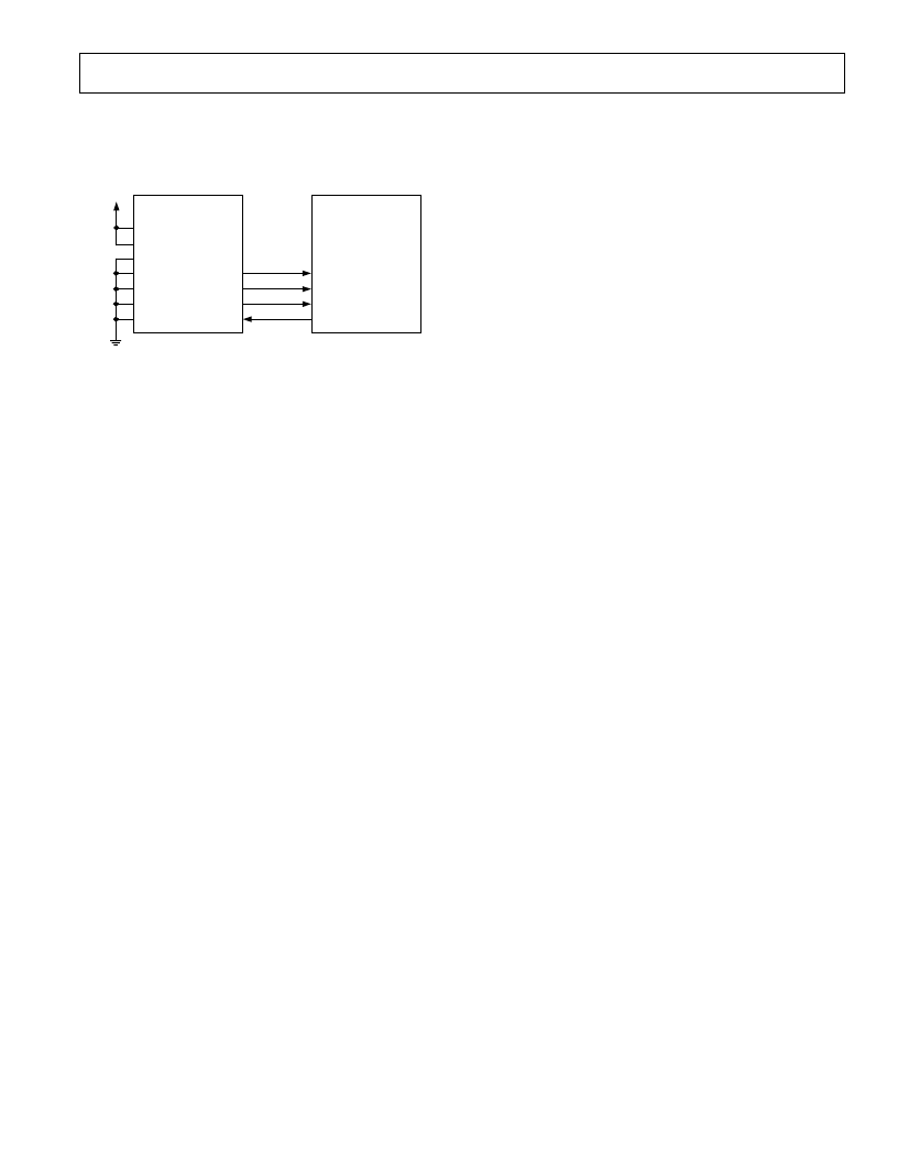
RFS
ADSP-21065L
*
SHARC
CNVST
AD7665
*
CS
SYNC
RD
EXT/
INT
DR
RCLK
FLAG OR TFS
SDOUT
SCLK
INVSYNC
INVSCLK
RDC/SDIN
SER/
PAR
DVDD
*
ADDITIONAL PINS OMITTED FOR CLARITY
Figure 23. Interfacing to the ADSP-21065L Using the
Serial Master Mode
APPLICATION HINTS
Layout
The AD7665 has very good immunity to noise on the power
supplies as can be seen in Figure 9. However, care should still
be taken with regard to grounding layout.
The printed circuit board that houses the AD7665 should be
designed so the analog and digital sections are separated and
confined to certain areas of the board. This facilitates the use of
ground planes that can be easily separated. Digital and analog
ground planes should be joined in only one place, preferably
underneath the AD7665, or, at least, as close as possible to the
AD7665. If the AD7665 is in a system where multiple devices
require analog-to-digital ground connections, the connection
should still be made at one point only, a star ground point,
which should be established as close as possible to the AD7665.
It is recommended to avoid running digital lines under the de-
vice as these will couple noise onto the die. The analog ground
plane should be allowed to run under the AD7665 to avoid
noise coupling. Fast switching signals like
CNVST
or clocks
should be shielded with digital ground to avoid radiating noise
to other sections of the board, and should never run near analog
signal paths. Crossover of digital and analog signals should be
avoided. Traces on different but close layers of the board should
run at right angles to each other. This will reduce the effect of
feedthrough through the board.
The power supply lines to the AD7665 should use as large a trace
as possible to provide low impedance paths and reduce the
effect of glitches on the power supply lines. Good decoupling is
also important to lower the supplies impedance presented to the
AD7665 and reduce the magnitude of the supply spikes. Decoupling
ceramic capacitors, typically 100 nF, should be placed on each
power supplies pins AVDD, DVDD and OVDD close to, and
ideally right up against these pins and their corresponding
ground pins. Additionally, low ESR 10
μ
F capacitors should be
located in the vicinity of the ADC to further reduce low fre-
quency ripple.
The DVDD supply of the AD7665 can be either a separate
supply or come from the analog supply, AVDD, or from the
digital interface supply, OVDD. When the system digital supply
is noisy, or fast switching digital signals are present, it is recom-
mended if no separate supply available, to connect the DVDD
digital supply to the analog supply AVDD through an RC filter
as shown in Figure 5, and connect the system supply to the
interface digital supply OVDD and the remaining digital cir-
cuitry. When DVDD is powered from the system supply, it is
useful to insert a bead to further reduce high-frequency spikes.
The AD7665 has five different ground pins; INGND, REFGND,
AGND, DGND, and OGND. INGND is used to sense the
analog input signal. REFGND senses the reference voltage and
should be a low impedance return to the reference because it
carries pulsed currents. AGND is the ground to which most
internal ADC analog signals are referenced. This ground must
be connected with the least resistance to the analog ground
plane. DGND must be tied to the analog or digital ground plane
depending on the configuration. OGND is connected to the
digital system ground.
The layout of the decoupling of the reference voltage is impor-
tant. The decoupling capacitor should be close to the ADC and
connected with short and large traces to minimize parasitic
inductances.
Evaluating the AD7665 Performance
A recommended layout for the AD7665 is outlined in the evalu-
ation board for the AD7665. The evaluation board package
includes a fully assembled and tested evaluation board, docu-
mentation, and software for controlling the board from a PC
via the Eval-Control Board.
相關PDF資料 |
PDF描述 |
|---|---|
| AD7665AST | 16-Bit, 570 kSPS CMOS ADC |
| AD7665ASTRL | 16-Bit, 570 kSPS CMOS ADC |
| AD7669AN | LC2MOS Complete, 8-Bit Analog I/0 Systems |
| AD7569TE | LC2MOS Complete, 8-Bit Analog I/0 Systems |
| AD7569KN | LC2MOS Complete, 8-Bit Analog I/0 Systems |
相關代理商/技術參數 |
參數描述 |
|---|---|
| AD7665ACP | 制造商:Analog Devices 功能描述:ADC Single SAR 570ksps 16-bit Parallel/Serial 48-Pin LFCSP EP 制造商:Rochester Electronics LLC 功能描述:16-BIT, 500 KSPS CMOS A/D CONVERTER - Bulk |
| AD7665ACPRL | 制造商:Analog Devices 功能描述:ADC Single SAR 570ksps 16-bit Parallel/Serial 48-Pin LFCSP EP T/R |
| AD7665ACPZ | 功能描述:IC ADC 16BIT CMOS 5V 48LFCSP RoHS:是 類別:集成電路 (IC) >> 數據采集 - 模數轉換器 系列:PulSAR® 標準包裝:1 系列:- 位數:14 采樣率(每秒):83k 數據接口:串行,并聯 轉換器數目:1 功率耗散(最大):95mW 電壓電源:雙 ± 工作溫度:0°C ~ 70°C 安裝類型:通孔 封裝/外殼:28-DIP(0.600",15.24mm) 供應商設備封裝:28-PDIP 包裝:管件 輸入數目和類型:1 個單端,雙極 |
| AD7665ACPZRL | 功能描述:IC ADC 16BIT CMOS 5V 48LFCSP RoHS:是 類別:集成電路 (IC) >> 數據采集 - 模數轉換器 系列:PulSAR® 標準包裝:1 系列:- 位數:14 采樣率(每秒):83k 數據接口:串行,并聯 轉換器數目:1 功率耗散(最大):95mW 電壓電源:雙 ± 工作溫度:0°C ~ 70°C 安裝類型:通孔 封裝/外殼:28-DIP(0.600",15.24mm) 供應商設備封裝:28-PDIP 包裝:管件 輸入數目和類型:1 個單端,雙極 |
| AD7665AST | 制造商:Rochester Electronics LLC 功能描述: 制造商:Analog Devices 功能描述:Analog-Digital Converter IC Number of Bi |
發布緊急采購,3分鐘左右您將得到回復。