- 您現在的位置:買賣IC網 > PDF目錄373913 > AD7677ASTRL (ANALOG DEVICES INC) 16-Bit, 1 LSB INL, 1 MSPS Differential ADC PDF資料下載
參數資料
| 型號: | AD7677ASTRL |
| 廠商: | ANALOG DEVICES INC |
| 元件分類: | ADC |
| 英文描述: | 16-Bit, 1 LSB INL, 1 MSPS Differential ADC |
| 中文描述: | 1-CH 16-BIT SUCCESSIVE APPROXIMATION ADC, SERIAL/PARALLEL ACCESS, PQFP48 |
| 封裝: | LQFP-48 |
| 文件頁數: | 11/20頁 |
| 文件大小: | 322K |
| 代理商: | AD7677ASTRL |
REV. 0
AD7677
–11–
TEMPERATURE
–
C
250
P
–
0
–
55
100
–
15
105
45
150
50
DVDD
–
35
5
85
25
65
200
OVDD
AVDD
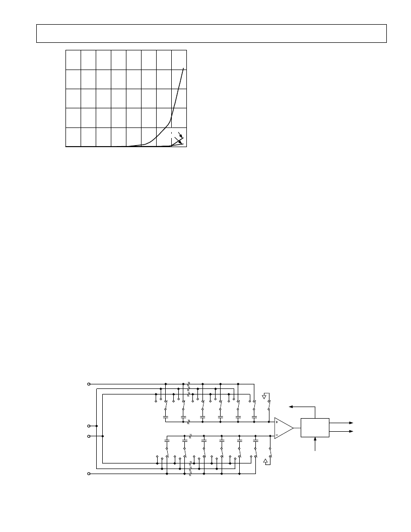
TPC 13. Power-Down Operating Currents vs. Temperature
CIRCUIT INFORMATION
The AD7677 is a very fast, low-power, single-supply, precise,
16-bit analog-to-digital converter (ADC). The AD7677 features
different modes to optimize performances according to the
applications.
In Warp mode, the AD7677 is capable of converting 1,000,000
samples per second (1 MSPS).
The AD7677 provides the user with an on-chip track/hold,
successive approximation ADC that does not exhibit any pipe-
line or latency, making it ideal for multiple multiplexed channel
applications.
The AD7677 can be operated from a single 5 V supply and
be interfaced to either 5 V or 3 V digital logic. It is housed in a
48-lead LQFP package that combines space savings and flexible
configurations as either serial or parallel interface. The AD7677
is a pin-to-pin-compatible upgrade of the AD7664, AD7675,
and AD7676.
CONVERTER OPERATION
The AD7677 is a successive approximation analog-to-digital
converter based on a charge redistribution DAC. Figure 3 shows
the simplified schematic of the ADC. The capacitive DAC con-
sists of two identical arrays of 16 binary weighted capacitors
that are connected to the two comparator inputs.
During the acquisition phase, terminals of the array tied to the
comparator’s input are connected to AGND via SW
+
and SW
–
.
All independent switches are connected to the analog inputs.
Thus, the capacitor arrays are used as sampling capacitors and
acquire the analog signal on IN+ and IN– inputs. When the
acquisition phase is complete and the
CNVST
input goes
low, a conversion phase is initiated. When the conversion phase
begins, SW
+
and SW
–
are opened first. The two capacitor arrays
are then disconnected from the inputs and connected to the
REFGND input. Therefore, the differential voltage between the
inputs IN+ and IN– captured at the end of the acquisition phase
is applied to the comparator inputs, causing the comparator to
become unbalanced. By switching each element of the capacitor
array between REFGND or REF, the comparator input varies
by binary weighted voltage steps (V
REF
/2, V
REF
/4 . . . V
REF
/65536).
The control logic toggles these switches, starting with the MSB
first, in order to bring the comparator back into a balanced
condition. After the completion of this process, the control logic
generates the ADC output code and brings BUSY output low.
Modes of Operation
The AD7677 features three modes of operations, Warp, Normal,
and Impulse. Each of these modes is more suitable for specific
applications.
The Warp mode allows the fastest conversion rate up to 1 MSPS.
However, in this mode, and this mode only, the full specified accu-
racy is guaranteed only when the time between conversion does
not exceed 1 ms. If the time between two consecutive conversions
is longer than 1 ms, for instance, after power-up, the first conver-
sion result should be ignored. This mode makes the AD7677
ideal for applications where fast sample rates are required.
The Normal mode is the fastest mode (800 kSPS) without any
limitation about the time between conversions. This mode makes
the AD7677 ideal for asynchronous applications such as data
acquisition systems, where both high accuracy and fast sample
rate are required.
The Impulse mode, the lowest power dissipation mode, allows
power saving between conversions. The maximum throughput
in this mode is 666 kSPS. When operating at 100 SPS, for
example, it typically consumes only 15
μ
W. This feature makes
the AD7677 ideal for battery-powered applications.
IN+
REF
REFGND
IN
–
32,768C 16,384C
MSB
4C
2C
C
C
LSB
SW+
SWITCHES
CONTROL
32,768C 16,384C
MSB
4C
2C
C
C
LSB
SW
–
BUSY
OUTPUT
CODE
CNVST
CONTROL
LOGIC
COMP
Figure 3. ADC Simplified Schematic
相關PDF資料 |
PDF描述 |
|---|---|
| AD7679CB1 | 18-Bit, 2.5 LSB INL, 570 kSPS SAR ADC |
| AD7694 | 16-Bit, 250 kSPS PulSAR ADC in MSOP |
| AD7694ARM | 16-Bit, 250 kSPS PulSAR ADC in MSOP |
| AD7694ARMRL7 | 16-Bit, 250 kSPS PulSAR ADC in MSOP |
| AD7694BRM | 16-Bit, 250 kSPS PulSAR ADC in MSOP |
相關代理商/技術參數 |
參數描述 |
|---|---|
| AD7677ASTZ | 功能描述:IC ADC 16BIT 1MSPS DIFF 48-LQFP RoHS:是 類別:集成電路 (IC) >> 數據采集 - 模數轉換器 系列:PulSAR® 標準包裝:1 系列:microPOWER™ 位數:8 采樣率(每秒):1M 數據接口:串行,SPI? 轉換器數目:1 功率耗散(最大):- 電壓電源:模擬和數字 工作溫度:-40°C ~ 125°C 安裝類型:表面貼裝 封裝/外殼:24-VFQFN 裸露焊盤 供應商設備封裝:24-VQFN 裸露焊盤(4x4) 包裝:Digi-Reel® 輸入數目和類型:8 個單端,單極 產品目錄頁面:892 (CN2011-ZH PDF) 其它名稱:296-25851-6 |
| AD7677ASTZ | 制造商:Analog Devices 功能描述:IC 16-BIT ADC |
| AD7677ASTZRL | 功能描述:IC ADC 16BIT 1MSPS DIFF 48-LQFP RoHS:是 類別:集成電路 (IC) >> 數據采集 - 模數轉換器 系列:PulSAR® 標準包裝:1 系列:- 位數:14 采樣率(每秒):83k 數據接口:串行,并聯 轉換器數目:1 功率耗散(最大):95mW 電壓電源:雙 ± 工作溫度:0°C ~ 70°C 安裝類型:通孔 封裝/外殼:28-DIP(0.600",15.24mm) 供應商設備封裝:28-PDIP 包裝:管件 輸入數目和類型:1 個單端,雙極 |
| AD7678 | 制造商:AD 制造商全稱:Analog Devices 功能描述:18-Bit, 2.5 LSB INL, 570 kSPS SAR ADC |
| AD7678ACP | 制造商:Analog Devices 功能描述:ADC Single SAR 100ksps 18-bit Parallel/Serial 48-Pin LFCSP EP 制造商:Rochester Electronics LLC 功能描述:18-BIT,100KSPSSARADC - Bulk 制造商:Analog Devices 功能描述:18BIT SAR ADC SMD 7678 LFSCP-48 |
發布緊急采購,3分鐘左右您將得到回復。