- 您現(xiàn)在的位置:買賣IC網(wǎng) > PDF目錄373913 > AD7677ASTRL (ANALOG DEVICES INC) 16-Bit, 1 LSB INL, 1 MSPS Differential ADC PDF資料下載
參數(shù)資料
| 型號(hào): | AD7677ASTRL |
| 廠商: | ANALOG DEVICES INC |
| 元件分類: | ADC |
| 英文描述: | 16-Bit, 1 LSB INL, 1 MSPS Differential ADC |
| 中文描述: | 1-CH 16-BIT SUCCESSIVE APPROXIMATION ADC, SERIAL/PARALLEL ACCESS, PQFP48 |
| 封裝: | LQFP-48 |
| 文件頁數(shù): | 14/20頁 |
| 文件大小: | 322K |
| 代理商: | AD7677ASTRL |
REV. 0
AD7677
–14–
Voltage Reference Input
The AD7677 uses an external 2.5 V voltage reference. The
voltage reference input REF of the AD7677 has a dynamic
input impedance. Therefore, it should be driven by a low
impedance source with an efficient decoupling between REF
and REFGND inputs. This decoupling depends on the choice
of the voltage reference, but usually consists of a 1
μ
F ceramic
capacitor and a low ESR tantalum capacitor connected to the
REF and REFGND inputs with minimum parasitic inductance.
47
μ
F is an appropriate value for the tantalum capacitor when
used with one of the recommended reference voltages:
The lownoise, low temperature drift ADR421 and AD780
voltage references
The lowpower ADR291 voltage reference
The lowcost AD1582 voltage reference
For applications using multiple AD7677s, it is more effective
to buffer the reference voltage with a lownoise, very stable op
amp like the AD8031.
Care should also be taken with the reference temperature coeffi-
cient of the voltage reference which directly affects the full-scale
accuracy if this parameter matters. For instance, a
±
15 ppm/
°
C
tempco of the reference changes the full scale by
±
1 LSB/
°
C.
Note that V
REF
, as mentioned in the specification table, could be
increased to AVDD – 1.85 V. Since the input range is defined
in terms of V
REF
, this would essentially increase the range to
make it a
±
3 V input range with a reference voltage of 3 V. One
of the benefits here is the increased SNR obtained as a result of
this increase. The theoretical improvement as a result of this
increase in reference is 1.58 dB (20 log [3/2.5]). Due to the
theoretical quantization noise however, the observed improve-
ment is approximately 1 dB. The AD780 can be selected with a
3 V reference voltage.
FREQUENCY
–
Hz
75
P
–
35
65
10k
10M
1k
1M
55
100k
45
70
60
50
40
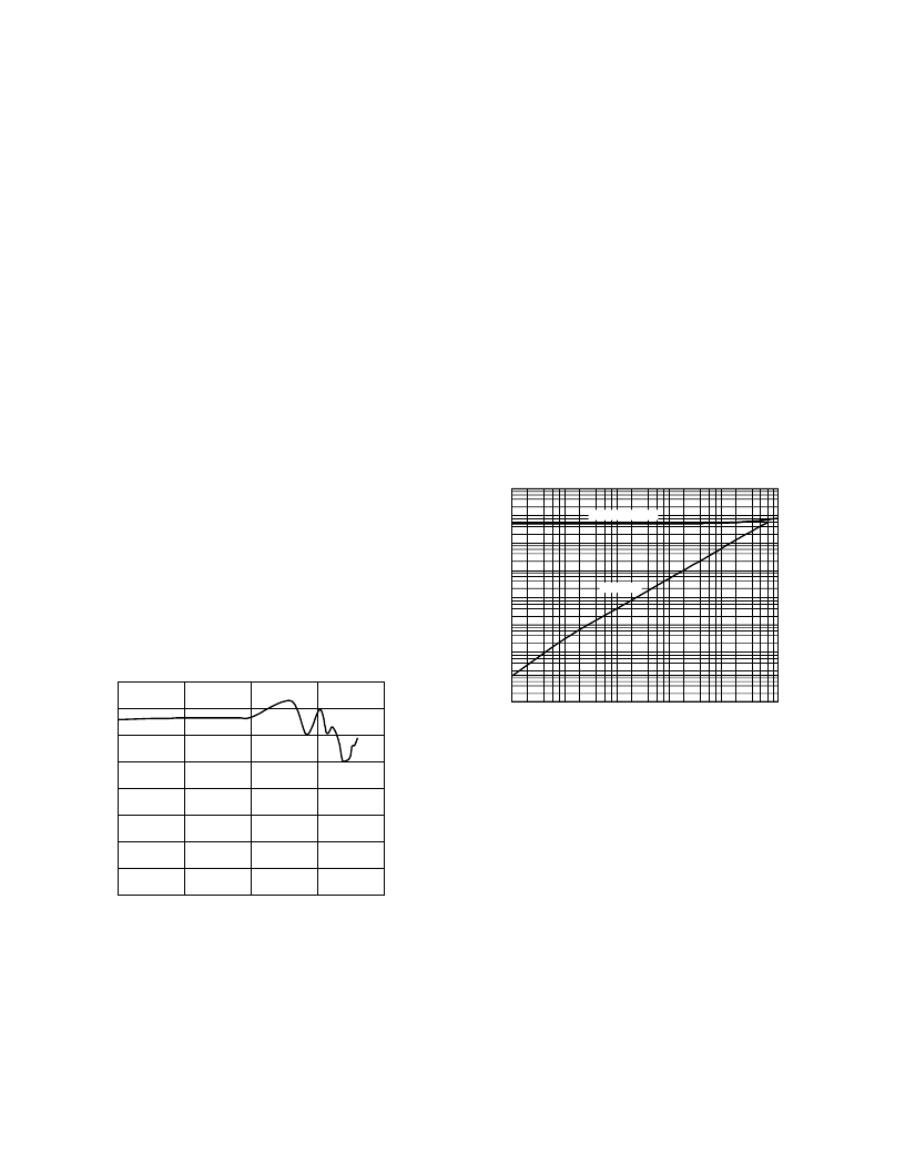
Figure 9. PSRR vs. Frequency
Power Supply
The AD7677 uses three sets of power supply pins: an analog
5 V supply AVDD, a digital 5 V core supply DVDD, and a
digital input/output interface supply OVDD. The OVDD supply
allows direct interface with any logic working between 2.7 V and
5.25 V. To reduce the number of supplies needed, the digital
core (DVDD) can be supplied through a simple RC filter from
the analog supply as shown in Figure 5. The AD7677 is inde-
pendent of power supply sequencing and thus free from supply
voltage induced latchup. Additionally, it is very insensitive to
power supply variations over a wide frequency range as shown
in Figure 9.
POWER DISSIPATION
In Impulse mode, the AD7677 automatically reduces its power
consumption at the end of each conversion phase. During the
acquisition phase, the operating currents are very low which
allows a significant power saving when the conversion rate is
reduced as shown in Figure 10. This feature makes the AD7677
ideal for very low-power battery applications.
It should be noted that the digital interface remains active even
during the acquisition phase. To reduce the operating digital
supply currents even further, the digital inputs need to be driven
close to the power rails (i.e., DVDD and DGND) and OVDD
should not exceed DVDD by more than 0.3 V.
SAMPLING RATE
–
SPS
1M
P
–
0.1
10k
100
100k
10
10k
100
1k
1
100k
1k
10
1M
WARP/NORMAL
IMPULSE
Figure 10. Power Dissipation vs. Sample Rate
CONVERSION CONTROL
Figure 11 shows the detailed timing diagrams of the conversion
process. The AD7677 is controlled by the signal
CNVST
which
initiates conversion. Once initiated, it cannot be restarted or
aborted, even by the power-down input PD, until the conver-
sion is complete. The
CNVST
signal operates independently of
CS
and
RD
signals.
In Impulse mode, conversions can be automatically initiated. If
CNVST
is held low when BUSY is low, the AD7677 controls
the acquisition phase and then automatically initiates a new
conversion. By keeping
CNVST
low, the AD7677 keeps the
conversion process running by itself. It should be noted that the
相關(guān)PDF資料 |
PDF描述 |
|---|---|
| AD7679CB1 | 18-Bit, 2.5 LSB INL, 570 kSPS SAR ADC |
| AD7694 | 16-Bit, 250 kSPS PulSAR ADC in MSOP |
| AD7694ARM | 16-Bit, 250 kSPS PulSAR ADC in MSOP |
| AD7694ARMRL7 | 16-Bit, 250 kSPS PulSAR ADC in MSOP |
| AD7694BRM | 16-Bit, 250 kSPS PulSAR ADC in MSOP |
相關(guān)代理商/技術(shù)參數(shù) |
參數(shù)描述 |
|---|---|
| AD7677ASTZ | 功能描述:IC ADC 16BIT 1MSPS DIFF 48-LQFP RoHS:是 類別:集成電路 (IC) >> 數(shù)據(jù)采集 - 模數(shù)轉(zhuǎn)換器 系列:PulSAR® 標(biāo)準(zhǔn)包裝:1 系列:microPOWER™ 位數(shù):8 采樣率(每秒):1M 數(shù)據(jù)接口:串行,SPI? 轉(zhuǎn)換器數(shù)目:1 功率耗散(最大):- 電壓電源:模擬和數(shù)字 工作溫度:-40°C ~ 125°C 安裝類型:表面貼裝 封裝/外殼:24-VFQFN 裸露焊盤 供應(yīng)商設(shè)備封裝:24-VQFN 裸露焊盤(4x4) 包裝:Digi-Reel® 輸入數(shù)目和類型:8 個(gè)單端,單極 產(chǎn)品目錄頁面:892 (CN2011-ZH PDF) 其它名稱:296-25851-6 |
| AD7677ASTZ | 制造商:Analog Devices 功能描述:IC 16-BIT ADC |
| AD7677ASTZRL | 功能描述:IC ADC 16BIT 1MSPS DIFF 48-LQFP RoHS:是 類別:集成電路 (IC) >> 數(shù)據(jù)采集 - 模數(shù)轉(zhuǎn)換器 系列:PulSAR® 標(biāo)準(zhǔn)包裝:1 系列:- 位數(shù):14 采樣率(每秒):83k 數(shù)據(jù)接口:串行,并聯(lián) 轉(zhuǎn)換器數(shù)目:1 功率耗散(最大):95mW 電壓電源:雙 ± 工作溫度:0°C ~ 70°C 安裝類型:通孔 封裝/外殼:28-DIP(0.600",15.24mm) 供應(yīng)商設(shè)備封裝:28-PDIP 包裝:管件 輸入數(shù)目和類型:1 個(gè)單端,雙極 |
| AD7678 | 制造商:AD 制造商全稱:Analog Devices 功能描述:18-Bit, 2.5 LSB INL, 570 kSPS SAR ADC |
| AD7678ACP | 制造商:Analog Devices 功能描述:ADC Single SAR 100ksps 18-bit Parallel/Serial 48-Pin LFCSP EP 制造商:Rochester Electronics LLC 功能描述:18-BIT,100KSPSSARADC - Bulk 制造商:Analog Devices 功能描述:18BIT SAR ADC SMD 7678 LFSCP-48 |
發(fā)布緊急采購,3分鐘左右您將得到回復(fù)。