- 您現(xiàn)在的位置:買賣IC網 > PDF目錄373974 > AD7699 (Analog Devices, Inc.) 16-Bit, 8-Channel, 250 kSPS PulSAR㈢ ADC. PDF資料下載
參數(shù)資料
| 型號: | AD7699 |
| 廠商: | Analog Devices, Inc. |
| 英文描述: | 16-Bit, 8-Channel, 250 kSPS PulSAR㈢ ADC. |
| 中文描述: | 16位,8通道,250 kSPS的PulSAR系列㈢ADC的。 |
| 文件頁數(shù): | 13/20頁 |
| 文件大小: | 2041K |
| 代理商: | AD7699 |
Preliminary Technical Data
AD7689
CONFIGURATION REGISTER, CFG
The AD7689 uses a 14-bit configuration register (CFG[13:0])
for configuring the inputs, channel to be converted, 1-pole filter
bandwidth, reference, and channel sequencer. The CFG is
latched MSB first with DIN synchronized to SCK rising edge. At
the end of conversion, the register is updated allowing the new
settings to be used. There is always a one deep conversion delay
regardless of when the CFG is written to; during or after
conversion. Note that at power up, the CFG is undefined and a
dummy conversion is required to update the register. To preload
the CFG with a factory setting, hold DIN high for 1 conversion.
Thus CFG[13:0] = 0x3FFF. This sets the AD7689 for:
IN[7:0] unipolar referenced to GND, sequenced in order
Full bandwidth for 1-pole filter
Internal reference/temp sensor disabled, buffer enabled
No read back of CFG
Table 9 Summarizes the configuration register bit details. Each
corresponding section, where necessary, highlights further
details of the bits used for the specific functions.
Table 9. Configuration Register Description
Bit
Name
Description
13
CFG
0 – Keep current config settings
1 – Overwrite contents of register
12:10
INCC
Input Channel Configuration
12
11
10
0
0
X
Rev. PrC | Page 13 of 20
Function
Bipolar differential pairs, IN-
referenced to V
REF
/2
Bipolar, IN0-IN7 referenced to
COM = V
REF
/2
Temperature sensor
Unipolar differential pairs, IN-
referenced to GND (±100mV)
Unipolar, IN0-IN7 referenced to
COM = GND (±100mV)
Unipolar, IN0-IN7 referenced to
GND (single ended)
0
1
0
0
1
1
0
1
X
1
1
0
1
1
1
Channel Selection in binary fashion
9
8
7
Function
0
0
0
IN0
0
0
1
IN1
.
.
.
1
1
1
IN7
Selects BW for Low Pass Filter
0 – of BW
1 – Full BW
Reference/Buffer Selection
5
4
3
Function
0
0
0
Internal ref, REF = 2.5V output
0
0
1
Internal ref, REF = 4.096V output
0
1
0
External ref, Temp enabled
0
1
1
External ref, internal Buffer,
Temp enabled
1
1
0
External ref, Temp disabled
1
1
1
External ref, internal Buf, Temp
disabled
9:7
INn
6
BW
5:3
REF
2:1
SEQ
Channel Sequencer
2
1
0
0
0
1
1
0
Function
Disable Sequencer
Update config during sequence
Scan IN0–INn (set in CFG[9:7])
then TEMP
Scan IN0–INn (set in CFG[9:7])
Read back
0 – Read back current configuration at end of data
1- Do not read back contents of configuration
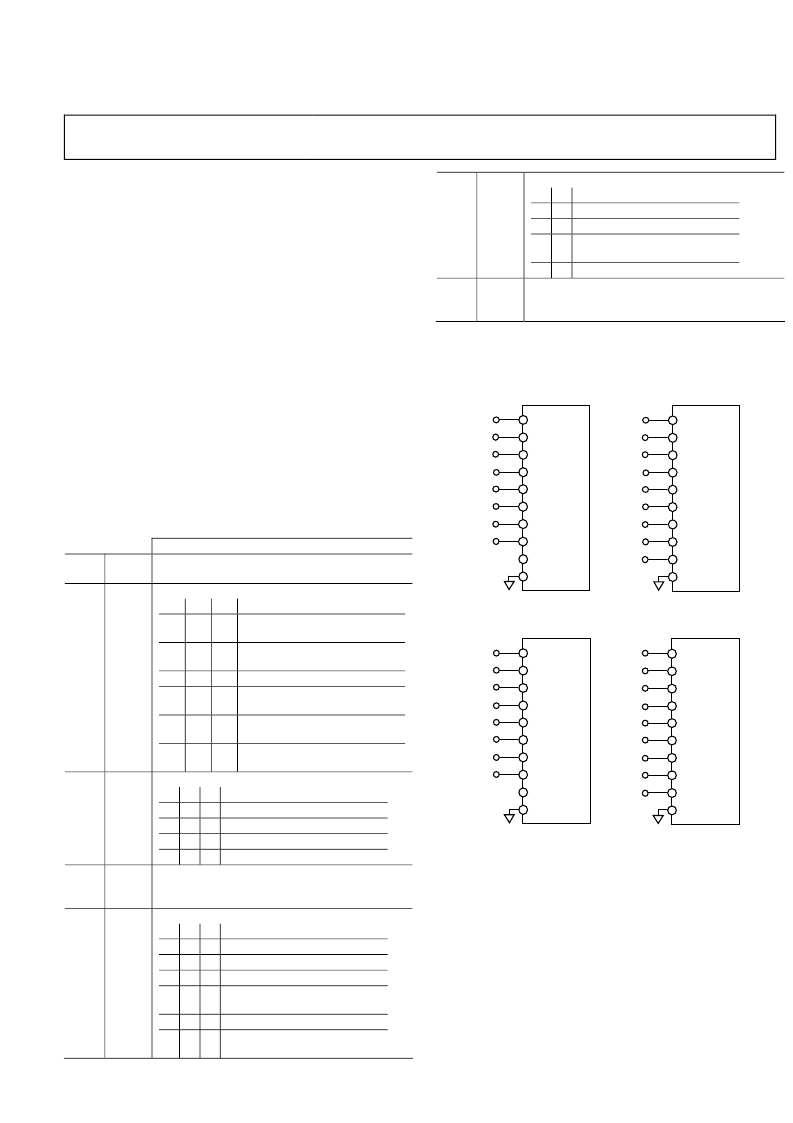
ANALOG INPUTS
Input Configurations
Figure 14 shows the different methods for configuring the
analog inputs with CFG[12:10].
1
1
0
RB
GND
-
COM
CH0+
CH3+
CH1+
CH2+
CH4+
CH5+
CH6+
CH7+
CH0+
CH3+
CH1+
CH2+
CH4+
CH5+
CH6+
CH7+
COM-
GND
COM
IN1
IN0
IN2
IN3
IN4
IN5
IN6
IN7
IN1
IN0
IN2
IN3
IN4
IN5
IN6
IN7
IN1
IN0
IN2
IN3
IN4
IN5
IN6
IN7
IN1
IN0
IN2
IN3
IN4
IN5
IN6
IN7
A- 8 CHANNELS,
SINGLE ENDED
B - 8 CHANNELS,
COMMON REFERNCE
GND
COM
CH0+ (-)
CH1+ (-)
CH2+ (-)
CH3+ (-)
CH0- (+)
CH1- (+)
CH0+ (-)
CH1+ (-)
CH0- (+)
CH1- (+)
CH2- (+)
CH3- (+)
C - 4 CHANNELS,
DIFFERENTIAL
GND
COM
CH2+
CH3+
CH4+
CH5+
D - COMBINATION
COM-
{
{
{
{
{
{
Figure 14. Multiplexed Analog Input Configuraitons
The analog inputs can be configured as:
Figure 14A, single ended referenced to system ground;
CFG[12:10] = 111
2
.
Figure 14B, bipolar differential with a common reference
point, COM, = V
REF
/2; CFG[12:10] = 010
2
.
Unipolar differential with COM connected to a ground
sense; CFG[12:10] = 110
2
.
Figure 14C, bipolar differential pairs with INx- referenced
to V
REF
/2; CFG[12:10] = 00X
2
.
Unipolar differential pairs with INx- referenced to a
相關PDF資料 |
PDF描述 |
|---|---|
| ADA4851-4 | Low Cost, High Speed, Rail-to-Rail, Output Op Amps |
| ADA4851-2 | Low Cost, High Speed, Rail-to-Rail, Output Op Amps |
| ADA4899-1 | Unity Gain Stable, Ultralow Distortion, 1 nV/ Hz Voltage Noise, High Speed Op Amp |
| ADA4899-1YCPZ-R2 | Unity Gain Stable, Ultralow Distortion, 1 nV/ Hz Voltage Noise, High Speed Op Amp |
| ADA4899-1YCPZ-R7 | Unity Gain Stable, Ultralow Distortion, 1 nV/ Hz Voltage Noise, High Speed Op Amp |
相關代理商/技術參數(shù) |
參數(shù)描述 |
|---|---|
| AD7699BCBZ-RL7 | 功能描述:8 CH 500KSPS 16BIT ADC IC 制造商:analog devices inc. 系列:* 包裝:剪切帶(CT) 零件狀態(tài):在售 封裝/外殼:20-UFBGA,WLCSP 供應商器件封裝:20-WLCSP(2.39x2.39) 標準包裝:1 |
| AD7699BCPZ | 功能描述:IC ADC 8CH 16BIT 500KSPS 20LFCSP RoHS:是 類別:集成電路 (IC) >> 數(shù)據(jù)采集 - 模數(shù)轉換器 系列:- 標準包裝:1 系列:microPOWER™ 位數(shù):8 采樣率(每秒):1M 數(shù)據(jù)接口:串行,SPI? 轉換器數(shù)目:1 功率耗散(最大):- 電壓電源:模擬和數(shù)字 工作溫度:-40°C ~ 125°C 安裝類型:表面貼裝 封裝/外殼:24-VFQFN 裸露焊盤 供應商設備封裝:24-VQFN 裸露焊盤(4x4) 包裝:Digi-Reel® 輸入數(shù)目和類型:8 個單端,單極 產品目錄頁面:892 (CN2011-ZH PDF) 其它名稱:296-25851-6 |
| AD7699BCPZRL7 | 功能描述:IC ADC 8CH 16BIT 500KSPS 20LFCSP RoHS:是 類別:集成電路 (IC) >> 數(shù)據(jù)采集 - 模數(shù)轉換器 系列:- 標準包裝:1,000 系列:- 位數(shù):12 采樣率(每秒):300k 數(shù)據(jù)接口:并聯(lián) 轉換器數(shù)目:1 功率耗散(最大):75mW 電壓電源:單電源 工作溫度:0°C ~ 70°C 安裝類型:表面貼裝 封裝/外殼:24-SOIC(0.295",7.50mm 寬) 供應商設備封裝:24-SOIC 包裝:帶卷 (TR) 輸入數(shù)目和類型:1 個單端,單極;1 個單端,雙極 |
| AD7701 | 制造商:AD 制造商全稱:Analog Devices 功能描述:LC2MOS 16-Bit A/D Converter |
| AD7701AN | 功能描述:IC ADC 16BIT LC2MOS 20-DIP RoHS:否 類別:集成電路 (IC) >> 數(shù)據(jù)采集 - 模數(shù)轉換器 系列:- 標準包裝:1 系列:- 位數(shù):14 采樣率(每秒):83k 數(shù)據(jù)接口:串行,并聯(lián) 轉換器數(shù)目:1 功率耗散(最大):95mW 電壓電源:雙 ± 工作溫度:0°C ~ 70°C 安裝類型:通孔 封裝/外殼:28-DIP(0.600",15.24mm) 供應商設備封裝:28-PDIP 包裝:管件 輸入數(shù)目和類型:1 個單端,雙極 |
發(fā)布緊急采購,3分鐘左右您將得到回復。