- 您現在的位置:買賣IC網 > PDF目錄373974 > AD7699 (Analog Devices, Inc.) 16-Bit, 8-Channel, 250 kSPS PulSAR㈢ ADC. PDF資料下載
參數資料
| 型號: | AD7699 |
| 廠商: | Analog Devices, Inc. |
| 英文描述: | 16-Bit, 8-Channel, 250 kSPS PulSAR㈢ ADC. |
| 中文描述: | 16位,8通道,250 kSPS的PulSAR系列㈢ADC的。 |
| 文件頁數: | 14/20頁 |
| 文件大小: | 2041K |
| 代理商: | AD7699 |
AD7689
Preliminary Technical Data
Rev. PrC | Page 14 of 20
ground sense; CFG[12:10] = 10X
2
.
In this configuration, the IN+ is identified by the channel
in CFG[9:7]. Example: for IN0 = IN1+ and IN1 = IN1-,
CFG[9:7] = 000
2
; for IN1 = IN1+ and IN0 = IN1-,
CFG[9:7] = 001
2
Figure 14D, sows the inputs configured in any of the above
combinations as the AD7689 can be configured
dynamically.
Sequencer
The AD7689 includes a channel sequencer useful for scanning
channels in a IN0 to INn fashion. Channels are scanned as
single or pairs and with or without the temperature sensor, after
the last channel is sequenced.
The sequencer starts with IN0 and finishes with INn set in
CFG[9:7]. For paired channels, the channels are paired
depending on the last channel set in CFG[9:7]. Note that the
channel pairs are always paired IN(even) = INx+ and IN(odd) =
INx- regardless of CFG[7].
To enable the sequencer, CFG[2:1] are written to for initializing
the sequencer. After CFG[13:0] is updated, DIN must be held
low while reading data out (at least for bit 13) or the CFG will
begin updating again.
While operating in a sequence, the CFG can be changed by
writing 01
2
to CFG[2:1]. However, if changing CFG[11] (paired
or single channel) or CFG[9:7] (last channel in sequence), the
sequence will reinitialize and convert IN0 (or IN1) after CFG is
updated.
Examples
(only bits for input and sequencer are highlighted)
Scan all IN[7:0] referenced to COM = GND sense with
temperature sensor:
13
CFG
-
12
11
INCC
1
10
9
8
7
6
BW
-
5
4
3
2
SEQ
1
1
0
RB
-
INn
1
REF
-
1
0
1
1
-
-
0
Scan 3 paired channels without temperature sensor and
referenced to V
REF
/2:
13
CFG
-
12
11
INCC
0
10
9
8
7
6
BW
-
5
4
3
2
SEQ
1
1
0
RB
-
INn
0
REF
-
0
X
1
X
-
-
1
Scan 4 paired channels referenced to a GND sense with
temperature sensor:
13
CFG
-
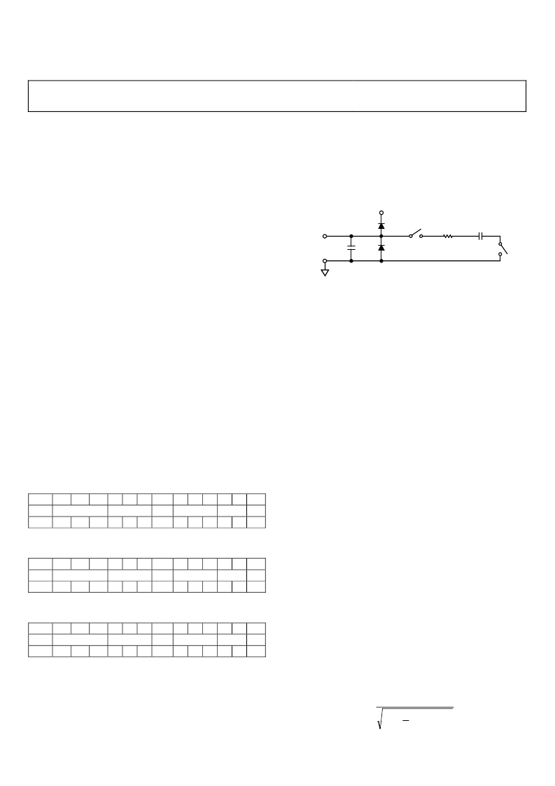
Input Structure
Figure 15 shows an equivalent circuit of the input structure of
the AD7689.
The two diodes, D1 and D2, provide ESD protection for the
analog inputs, IN[7:0] and COM. Care must be taken to ensure
that the analog input signal does not exceed the supply rails by
12
11
INCC
0
10
9
8
7
6
BW
-
5
4
3
2
SEQ
1
1
0
RB
-
INn
1
REF
-
1
X
1
X
-
-
0
more than 0.3 V because this causes the diodes to become
forward biased and to start conducting current. These diodes
can handle a forward-biased current of 130 mA maximum. For
instance, these conditions could eventually occur when the
input buffer’s supplies are different from VDD. In such a case,
for example, an input buffer with a short circuit, the current
limitation can be used to protect the part.
C
IN
R
IN
D1
D2
C
PIN
IN+
OR IN-
OR COM
GND
VDD
-
Figure 15. Equivalent Analog Input Circuit
The analog input structure allows the sampling of the true
differential signal between IN
n
+ and COM or IN
n
+ and IN
n
-.
By using these differential inputs, signals common to both
inputs are rejected.
During the acquisition phase, the impedance of the analog
inputs can be modeled as a parallel combination of the
capacitor, C
PIN
, and the network formed by the series
connection of R
IN
and C
IN
. C
PIN
is primarily the pin capacitance.
R
IN
is typically 3.5kΩ and is a lumped component made up of
serial resistors and the on resistance of the switches. C
IN
is
typically 27 pF and is mainly the ADC sampling capacitor.
Selectable Low Pass Filter
During the conversion phase, where the switches are opened,
the input impedance is limited to C
PIN
. While the AD7689 is
acquiring, R
IN
and C
IN
make a 1-pole, low-pass filter that reduces
undesirable aliasing effects and limits the noise from the driving
circuitry. The low pass filter can be programmed for the full
bandwidth or of the bandwidth with CFG[6] as shown in
Table 9.
DRIVER AMPLIFIER CHOICE
Although the AD7689 is easy to drive, the driver amplifier
needs to meet the following requirements:
The noise generated by the driver amplifier needs to be kept
as low as possible to preserve the SNR and transition noise
performance of the AD7689. Note that the AD7689 has a
noise much lower than most of the other 16-bit ADCs and,
therefore, can be driven by a noisier amplifier to meet a given
system noise specification. The noise coming from the
amplifier is filtered by the AD7689 analog input circuit low-
pass filter made by R
IN
and C
IN
or by an external filter, if one
is used. Because the typical noise of the AD7689 is 35 μV rms
(with V
REF
= 5V), the SNR degradation due to the amplifier is
+
=
2
3dB
2
)
(
f
2
π
35
35
20log
N
LOSS
Ne
SNR
相關PDF資料 |
PDF描述 |
|---|---|
| ADA4851-4 | Low Cost, High Speed, Rail-to-Rail, Output Op Amps |
| ADA4851-2 | Low Cost, High Speed, Rail-to-Rail, Output Op Amps |
| ADA4899-1 | Unity Gain Stable, Ultralow Distortion, 1 nV/ Hz Voltage Noise, High Speed Op Amp |
| ADA4899-1YCPZ-R2 | Unity Gain Stable, Ultralow Distortion, 1 nV/ Hz Voltage Noise, High Speed Op Amp |
| ADA4899-1YCPZ-R7 | Unity Gain Stable, Ultralow Distortion, 1 nV/ Hz Voltage Noise, High Speed Op Amp |
相關代理商/技術參數 |
參數描述 |
|---|---|
| AD7699BCBZ-RL7 | 功能描述:8 CH 500KSPS 16BIT ADC IC 制造商:analog devices inc. 系列:* 包裝:剪切帶(CT) 零件狀態:在售 封裝/外殼:20-UFBGA,WLCSP 供應商器件封裝:20-WLCSP(2.39x2.39) 標準包裝:1 |
| AD7699BCPZ | 功能描述:IC ADC 8CH 16BIT 500KSPS 20LFCSP RoHS:是 類別:集成電路 (IC) >> 數據采集 - 模數轉換器 系列:- 標準包裝:1 系列:microPOWER™ 位數:8 采樣率(每秒):1M 數據接口:串行,SPI? 轉換器數目:1 功率耗散(最大):- 電壓電源:模擬和數字 工作溫度:-40°C ~ 125°C 安裝類型:表面貼裝 封裝/外殼:24-VFQFN 裸露焊盤 供應商設備封裝:24-VQFN 裸露焊盤(4x4) 包裝:Digi-Reel® 輸入數目和類型:8 個單端,單極 產品目錄頁面:892 (CN2011-ZH PDF) 其它名稱:296-25851-6 |
| AD7699BCPZRL7 | 功能描述:IC ADC 8CH 16BIT 500KSPS 20LFCSP RoHS:是 類別:集成電路 (IC) >> 數據采集 - 模數轉換器 系列:- 標準包裝:1,000 系列:- 位數:12 采樣率(每秒):300k 數據接口:并聯 轉換器數目:1 功率耗散(最大):75mW 電壓電源:單電源 工作溫度:0°C ~ 70°C 安裝類型:表面貼裝 封裝/外殼:24-SOIC(0.295",7.50mm 寬) 供應商設備封裝:24-SOIC 包裝:帶卷 (TR) 輸入數目和類型:1 個單端,單極;1 個單端,雙極 |
| AD7701 | 制造商:AD 制造商全稱:Analog Devices 功能描述:LC2MOS 16-Bit A/D Converter |
| AD7701AN | 功能描述:IC ADC 16BIT LC2MOS 20-DIP RoHS:否 類別:集成電路 (IC) >> 數據采集 - 模數轉換器 系列:- 標準包裝:1 系列:- 位數:14 采樣率(每秒):83k 數據接口:串行,并聯 轉換器數目:1 功率耗散(最大):95mW 電壓電源:雙 ± 工作溫度:0°C ~ 70°C 安裝類型:通孔 封裝/外殼:28-DIP(0.600",15.24mm) 供應商設備封裝:28-PDIP 包裝:管件 輸入數目和類型:1 個單端,雙極 |
發布緊急采購,3分鐘左右您將得到回復。