- 您現在的位置:買賣IC網 > PDF目錄373913 > AD7701AQ (ANALOG DEVICES INC) LC2MOS 16-Bit A/D Converter PDF資料下載
參數資料
| 型號: | AD7701AQ |
| 廠商: | ANALOG DEVICES INC |
| 元件分類: | ADC |
| 英文描述: | LC2MOS 16-Bit A/D Converter |
| 中文描述: | 1-CH 16-BIT DELTA-SIGMA ADC, SERIAL ACCESS, CDIP20 |
| 封裝: | CERDIP-20 |
| 文件頁數: | 9/16頁 |
| 文件大小: | 312K |
| 代理商: | AD7701AQ |
–9–
REV. D
AD7701
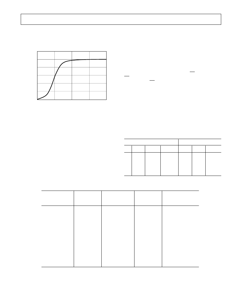
T he output settling of the AD7701 in response to a step input
change is shown in Figure 12. T he Gaussian response has fast
settling with no overshoot, and the worst-case settling time to
±
0.0007% (
±
0.5 LSB) is 125 ms with a 4.096 MHz master
clock frequency.
P
100
80
60
40
20
0
0
40
80
120
160
TIME – ms
Figure 12. AD7701 Step Response
USING T HE AD7701
SY ST E M DE SIGN CONSIDE RAT IONS
T he AD7701 operates differently from successive approxima-
tion ADCs or other integrating ADCs. Since it samples the sig-
nal continuously, like a tracking ADC, there is no need for a
start convert command. T he 16-bit output register is updated at
a 4 kHz rate, and the output can be read at any time, either syn-
chronously or asynchronously.
C LOC K ING
T he AD7701 requires a master clock input, which may be an
external T T L/CMOS compatible clock signal applied to the
CLK IN pin (CLK OUT not used). Alternatively, a crystal of the
correct frequency can be connected between CLK IN and
CLK OUT , when the clock circuit will function as a crystal-
controlled oscillator.
T he input sampling frequency, output data rate, filter character-
istics and calibration time are all directly related to the master
clock frequency f
CLK IN
by the ratios given in the specification
table. T herefore, the first step in system design with the
AD7701 is to select a master clock frequency suitable for the
bandwidth and output data rate required by the application.
ANALOG INPUT RANGE S
T he AD7701 performs conversion relative to an externally
supplied reference voltage, which allows easy interfacing to
ratiometric systems. In addition, either unipolar or bipolar input
voltage range may be selected using the BP/
UP
input. With BP/
UP
tied low, the input range is unipolar and the span is 0 to
+V
REF
. With BP/
UP
tied high, the input range is bipolar and the
span is
±
V
REF
. In the bipolar mode both positive and negative
full scale are directly determined by V
REF
. T his offers superior
tracking of positive and negative full scale and better midscale
(bipolar zero) stability than bipolar schemes that simply scale
and offset the input range.
T he digital output coding for the unipolar range is Unipolar
Binary; for the bipolar range it is Offset Binary. Bit weights for
the unipolar and bipolar modes are shown in T able I. T he input
voltages and output codes for unipolar and bipolar ranges, using
the recommended +2.5 V reference, are shown in T able II.
T able I. Bit Weight T able (2.5 V Reference Voltage)
Unipolar Mode
Bipolar Mode
m
V
LSBs
% FS
ppm FS
LSBs
% FS
ppm FS
10
19
38
76
153
0.26
0.5
1.00
2.00
4.00
0.0004
0.0008
0.0015
0.0031
0.0061
4
8
15
31
61
0.13
0.26
0.5
1.00
2.00
0.0002
0.0004
0.0008
0.0015
0.0031
2
4
8
15
31
T able II. Output Coding
Unipolar Mode
Input Relative to
FS and AGND
Bipolar Mode
Input Relative to
FS and AGND
Input in Volts
Input in Volts
Output Data
1111 1111 1111 1111
1111 1111 1111 1110
1111 1111 1111 1101
1111 1111 1111 1100
+V
REF
– 1.5 LSB
+V
REF
– 2.5 LSB
+V
REF
– 3.5 LSB
+2.499943
+2.499905
+2.499867
+V
REF
– 1.5 LSB
+V
REF
– 2.5 LSB
+V
REF
– 3.5 LSB
+2.499886
+2.499810
+2.499733
1000 0000 0000 0001
1000 0000 0000 0000
0111 1111 1111 1111
0111 1111 1111 1110
+V
REF
/2 + 0.5 LSB
+V
REF
/2 – 0.5 LSB
+V
REF
/2 – 1.5 LSB
+1.250019
+1.249981
+1.249943
AGND + 0.5 LSB
AGND – 0.5 LSB
AGND – 1.5 LSB
+0.000038
–0.000038
–0.000114
0000 0000 0000 0011
0000 0000 0000 0010
0000 0000 0000 0001
0000 0000 0000 0000
AGND + 2.5 LSB
AGND + 1.5 LSB
AGND + 0.5 LSB
+0.000095
+0.000057
+0.000019
–V
REF
+ 2.5 LSB
–V
REF
+ 1.5 LSB
–V
REF
+ 0.5 LSB
–2.499810
–2.499886
–2.499962
NOT ES
1
V
= +2.5 V
2
AGND = 0 V
3
Unipolar Mode, 1 LSB = 2.5 V/655536 = 0.000038 V
4
Bipolar Mode, 1 LSB = 5 V/65536 = 0.000076 V
5
Inputs are voltages at code transitions.
相關PDF資料 |
PDF描述 |
|---|---|
| AD7701AR | LC2MOS 16-Bit A/D Converter |
| AD7701ARS | LC2MOS 16-Bit A/D Converter |
| AD7701BN | LC2MOS 16-Bit A/D Converter |
| AD7701BQ | LC2MOS 16-Bit A/D Converter |
| AD7701BR | LC2MOS 16-Bit A/D Converter |
相關代理商/技術參數 |
參數描述 |
|---|---|
| AD7701AR | 功能描述:IC ADC 16BIT LC2MOS 20-SOIC RoHS:否 類別:集成電路 (IC) >> 數據采集 - 模數轉換器 系列:- 標準包裝:1 系列:- 位數:14 采樣率(每秒):83k 數據接口:串行,并聯 轉換器數目:1 功率耗散(最大):95mW 電壓電源:雙 ± 工作溫度:0°C ~ 70°C 安裝類型:通孔 封裝/外殼:28-DIP(0.600",15.24mm) 供應商設備封裝:28-PDIP 包裝:管件 輸入數目和類型:1 個單端,雙極 |
| AD7701AR-REEL | 制造商:Rochester Electronics LLC 功能描述:- Tape and Reel |
| AD7701ARS | 功能描述:IC ADC 16BIT LC2MOS MONO 28-SSOP RoHS:否 類別:集成電路 (IC) >> 數據采集 - 模數轉換器 系列:- 標準包裝:1 系列:- 位數:14 采樣率(每秒):83k 數據接口:串行,并聯 轉換器數目:1 功率耗散(最大):95mW 電壓電源:雙 ± 工作溫度:0°C ~ 70°C 安裝類型:通孔 封裝/外殼:28-DIP(0.600",15.24mm) 供應商設備封裝:28-PDIP 包裝:管件 輸入數目和類型:1 個單端,雙極 |
| AD7701ARS-REEL | 功能描述:IC ADC 16BIT LC2MOS MONO 28-SSOP RoHS:否 類別:集成電路 (IC) >> 數據采集 - 模數轉換器 系列:- 標準包裝:1 系列:- 位數:14 采樣率(每秒):83k 數據接口:串行,并聯 轉換器數目:1 功率耗散(最大):95mW 電壓電源:雙 ± 工作溫度:0°C ~ 70°C 安裝類型:通孔 封裝/外殼:28-DIP(0.600",15.24mm) 供應商設備封裝:28-PDIP 包裝:管件 輸入數目和類型:1 個單端,雙極 |
| AD7701ARSZ | 功能描述:IC ADC 16BIT LC2MOS MONO 28SSOP RoHS:是 類別:集成電路 (IC) >> 數據采集 - 模數轉換器 系列:- 標準包裝:1 系列:- 位數:14 采樣率(每秒):83k 數據接口:串行,并聯 轉換器數目:1 功率耗散(最大):95mW 電壓電源:雙 ± 工作溫度:0°C ~ 70°C 安裝類型:通孔 封裝/外殼:28-DIP(0.600",15.24mm) 供應商設備封裝:28-PDIP 包裝:管件 輸入數目和類型:1 個單端,雙極 |
發布緊急采購,3分鐘左右您將得到回復。