- 您現在的位置:買賣IC網 > PDF目錄373913 > AD7701BQ (ANALOG DEVICES INC) LC2MOS 16-Bit A/D Converter PDF資料下載
參數資料
| 型號: | AD7701BQ |
| 廠商: | ANALOG DEVICES INC |
| 元件分類: | ADC |
| 英文描述: | LC2MOS 16-Bit A/D Converter |
| 中文描述: | 1-CH 16-BIT DELTA-SIGMA ADC, SERIAL ACCESS, CDIP20 |
| 封裝: | CERDIP-20 |
| 文件頁數: | 4/16頁 |
| 文件大小: | 312K |
| 代理商: | AD7701BQ |
AD7701
REV. D
–4–
ORDE RING GUIDE
T emperature
Range
Linearity
E rror (% FSR) Options*
Package
Model
AD7701AN
AD7701BN
AD7701AR
AD7701BR
AD7701ARS
AD7701AQ
AD7701BQ
AD7701SQ
AD7701T Q
–40
°
C to +85
°
C
–40
°
C to +85
°
C
–40
°
C to +85
°
C
–40
°
C to +85
°
C
–40
°
C to +85
°
C
–40
°
C to +85
°
C
–40
°
C to +85
°
C
–55
°
C to +125
°
C
–55
°
C to +125
°
C
0.003
0.0015
0.003
0.0015
0.003
0.003
0.0015
0.003
0.0015
N-20
N-20
R-20
R-20
RS-28
Q-20
Q-20
Q-20
Q-20
NOT ES
*N = Plastic DIP; Q = Cerdip; R = SOIC; RS = SSOP.
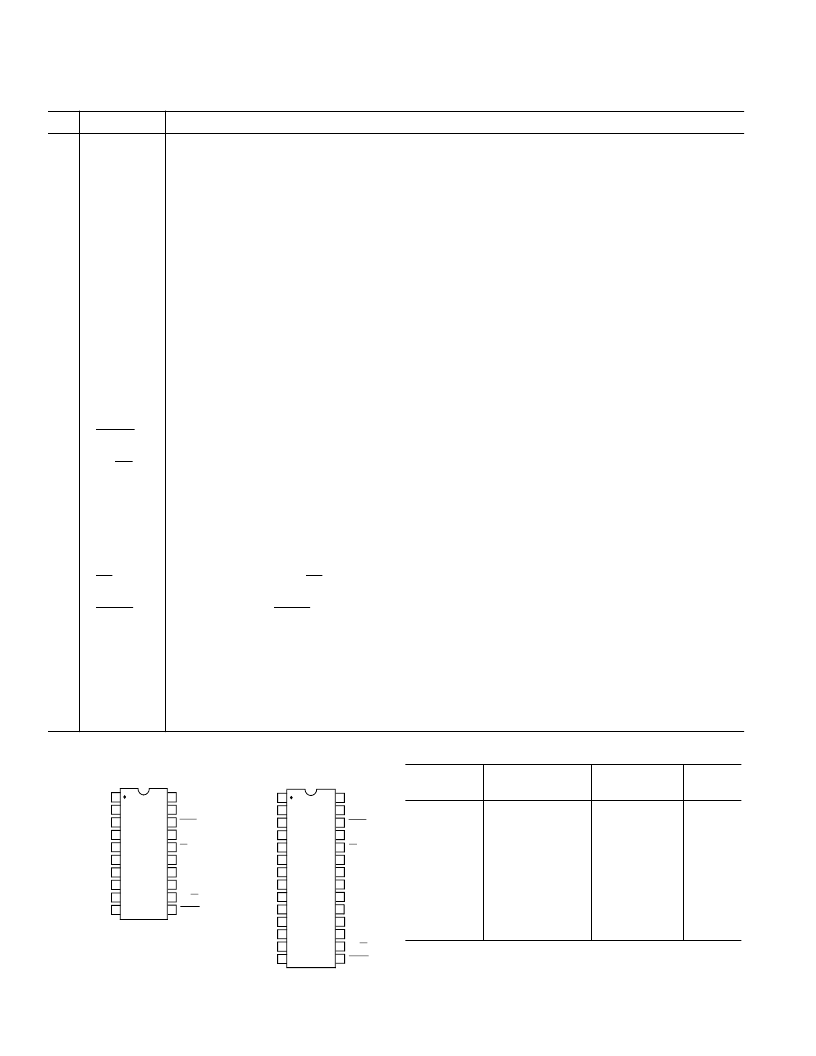
PIN FUNCT ION DE SCRIPT ION
Pin
Mnemonic
Description
1
MODE
Selects the Serial Interface Mode. If MODE is tied to –5 V, the AD7701 will operate in the asynchronous
communications (ac) mode. T he SCLK pin is configured as an input, and data is transmitted in two bytes,
each with one start bit and two stop bits. If MODE is tied to DGND, the synchronous external clocking
(SEC) mode is selected. SCLK is configured as an input, and the output appears without formatting, the
MSB coming first. If MODE is tied to +5 V, the AD7701 operates in the synchronous self-clocking (SSC)
mode. SCLK is configured as an output, with a clock frequency of f
CLK lN
/4 and 25% duty-cycle.
Clock Output to generate an Internal Master Clock by connecting a crystal between CLK OUT and CLK IN.
If an external clock is used, CLK OUT is not connected.
Clock Input for External Clock.
System Calibration Pins. T he state of these pins, when CAL is taken high, determines the type of calibration
performed.
Digital Ground. Ground reference for all digital signals.
Digital Negative Supply, –5 V nominal.
Analog Negative Supply, –5 V nominal.
Analog Ground. Ground reference for all analog signals.
Analog Input.
Voltage Reference Input, +2.5 V nominal. T his determines the value of positive full-scale in the unipolar
mode and of both positive and negative full-scale in the bipolar mode.
Sleep mode pin. When this pin is taken low, the AD7701 goes into a low-power mode with typically 10
μ
W
power consumption.
Bipolar/Unipolar Mode Pin. When this pin is low, the AD7701 is configured for a unipolar input range going
from AGND to V
REF
. When Pin 12 is high, the AD7701 is configured for a bipolar input range,
±
V
REF
.
Calibration Mode Pin. When CAL is taken high for more than 4 cycles, the AD7701 is reset and performs a
calibration cycle when CAL is brought low again. T he CAL pin can also be used as a strobe to synchronize
the operation of several AD7701s.
Analog Positive Supply, +5 V nominal.
Digital Positive Supply, +5 V nominal.
Chip Select Input. When
CS
is brought low, the AD7701 will begin to transmit serial data in a format deter-
mined by the state of the MODE pin.
Data Ready output.
DRDY
is low when valid data is available in the output register. It goes high after transmission
of a word is completed. It also goes high for four clock cycles when a new data word is being loaded into the out-
put register, to indicate that valid data is not available, irrespective of whether data transmission is complete or not.
Serial Clock Input/Output. T he SCLK pin in configured as an input or output, dependent on the type of se-
rial data transmission that has been selected by the MODE pin. When configured as an output in the syn-
chronous self-clocking mode, it has a frequency of f
CLK IN
/4 and a duty cycle of 25%.
Serial Data Output. T he AD7701’s output data is available at this pin as a 16-bit serial word. T he transmis-
sion format is determined by the state of the MODE pin.
2
CLK OUT
3
4, 17
CLK IN
SC1, SC2
5
6
7
8
9
10
DGND
DV
SS
AV
SS
AGND
A
IN
V
REF
11
SLEEP
12
BP/
UP
13
CAL
14
15
16
AV
DD
DV
DD
CS
18
DRDY
19
SCLK
20
SDAT A
DIP, C erdip, SOIC
MODE
SC1
DGND
CLKOUT
CLKIN
AGND
DV
SS
AV
SS
A
IN
V
REF
SDATA
SCLK
SC2
CAL
AV
DD
DV
DD
DRDY
CS
BP/UP
SLEEP
(TOP VIEW
AD7701
1
2
3
4
5
6
7
8
9
10
14
13
12
11
20
19
18
17
16
15
SSOP
MODE
SC1
DGND
CLKOUT
CLKIN
AGND
DV
SS
AV
SS
A
IN
V
REF
SDATA
SCLK
SC2
CAL
AV
DD
DV
DD
DRDY
CS
BP/UP
SLEEP
(TOP VIEW
AD7701
1
2
3
4
5
6
7
8
9
10
14
13
12
11
20
19
18
17
16
15
21
22
23
24
25
26
27
28
NC
NC
NC
NC
NC
NC
NC
NC
NC = NO CONNECT
PIN C ONF IGURAT IONS
相關PDF資料 |
PDF描述 |
|---|---|
| AD7701BR | LC2MOS 16-Bit A/D Converter |
| AD7701SQ | LC2MOS 16-Bit A/D Converter |
| AD7701TQ | LC2MOS 16-Bit A/D Converter |
| AD7701 | LC2MOS 16-Bit A/D Converter |
| AD7703 | LC2MOS 20-Bit A/D Converter |
相關代理商/技術參數 |
參數描述 |
|---|---|
| AD7701BR | 制造商:Analog Devices 功能描述:ADC Single Delta-Sigma 4ksps 16-bit Serial 20-Pin SOIC W 制造商:Rochester Electronics LLC 功能描述:16 BIT SIGMA DELTA CONVER - Bulk |
| AD7701BR-REEL | 制造商:Rochester Electronics LLC 功能描述: 制造商:Analog Devices 功能描述: |
| AD7701BRZ | 功能描述:IC ADC 16BIT LC2MOS MONO 20SOIC RoHS:是 類別:集成電路 (IC) >> 數據采集 - 模數轉換器 系列:- 其它有關文件:TSA1204 View All Specifications 標準包裝:1 系列:- 位數:12 采樣率(每秒):20M 數據接口:并聯 轉換器數目:2 功率耗散(最大):155mW 電壓電源:模擬和數字 工作溫度:-40°C ~ 85°C 安裝類型:表面貼裝 封裝/外殼:48-TQFP 供應商設備封裝:48-TQFP(7x7) 包裝:Digi-Reel® 輸入數目和類型:4 個單端,單極;2 個差分,單極 產品目錄頁面:1156 (CN2011-ZH PDF) 其它名稱:497-5435-6 |
| AD7701BRZ-REEL | 功能描述:IC ADC 16BIT LC2MOS 20SOIC RoHS:是 類別:集成電路 (IC) >> 數據采集 - 模數轉換器 系列:- 標準包裝:1 系列:- 位數:14 采樣率(每秒):83k 數據接口:串行,并聯 轉換器數目:1 功率耗散(最大):95mW 電壓電源:雙 ± 工作溫度:0°C ~ 70°C 安裝類型:通孔 封裝/外殼:28-DIP(0.600",15.24mm) 供應商設備封裝:28-PDIP 包裝:管件 輸入數目和類型:1 個單端,雙極 |
| AD7701SQ | 制造商:AD 制造商全稱:Analog Devices 功能描述:LC2MOS 16-Bit A/D Converter |
發布緊急采購,3分鐘左右您將得到回復。