- 您現在的位置:買賣IC網 > PDF目錄373913 > AD7701BQ (ANALOG DEVICES INC) LC2MOS 16-Bit A/D Converter PDF資料下載
參數資料
| 型號: | AD7701BQ |
| 廠商: | ANALOG DEVICES INC |
| 元件分類: | ADC |
| 英文描述: | LC2MOS 16-Bit A/D Converter |
| 中文描述: | 1-CH 16-BIT DELTA-SIGMA ADC, SERIAL ACCESS, CDIP20 |
| 封裝: | CERDIP-20 |
| 文件頁數: | 6/16頁 |
| 文件大小: | 312K |
| 代理商: | AD7701BQ |
AD7701
REV. D
–6–
1.6mA
200
μ
A
C
L
100pF
TO
OUTPUT
PIN
IOH
2.1V
+
I
OL
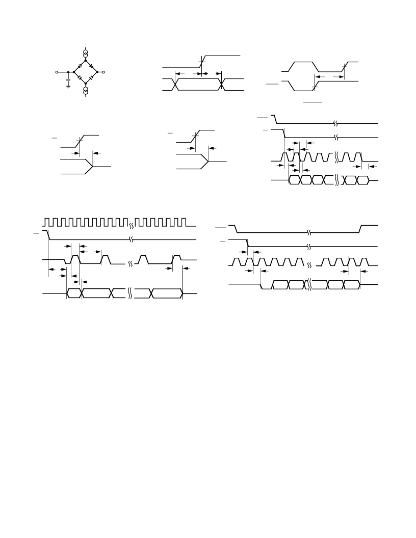
Figure 1. Load Circuit for Access
Time and Bus Relinquish Time
DATA
VALID
t
10
HI-Z
SDATA
CS
Figure 3. SSC Mode Data Hold
Time
CAL
SC1, SC2
SC1,SC2 VALID
t
1
t
2
Figure 2a. Calibration Control Timing
DATA
VALID
t
15
HI-Z
SDATA
CS
Figure 4a. SEC Mode Data Hold Time
CLKIN
SLEEP
t
3
Figure 2b.
SLEEP
Mode Timing
HI-Z
DB15
DB14
DB1
DB0
HI-Z
SDATA
DRDY
CS
t
12
t
11
t
13
t
14
SCLK
t
16
Figure 4b. SEC Mode Timing Diagram
T E RMINOLOGY
LINE ARIT Y E RROR
T his is the maximum deviation of any code from a straight line
passing through the endpoints of the transfer function. T he
endpoints of the transfer function are Zero-Scale (not to be
confused with Bipolar Zero), a point 0.5 LSB below the first
code transition (000 . . . 000 to 000 . . . 001) and Full-Scale, a
point 1.5 LSB above the last code transition (111 . . . 110 to
111 . . . 111). T he error is expressed as a percentage of full
scale.
DIFFE RE NT IAL LINE ARIT Y E RROR
T his is the difference between any code’s actual width and the
ideal (1 LSB) width. Differential Linearity Error is expressed in
LSBs. A differential linearity specification of
±
1 LSB or less
guarantees monotonicity.
POSIT IVE FULL-SCALE E RROR
Positive Full-Scale Error is the deviation of the last code
transition (111 . . . 110 to 111 . . . 111) from the ideal (V
REF
–3/2 LSBs). It applies to both positive and negative analog input
ranges and it is expressed in microvolts.
UNIPOLAR OFFSE T E RROR
Unipolar Offset Error is the deviation of the first code transition
from the ideal (AGND + 0.5 LSB) when operating in the uni-
polar mode. It is expressed in microvolts.
BIPOLAR ZE RO E RROR
T his is the deviation of the midscale transition (0111 . . . 111 to
1000 . . . 000) from the ideal (AGND – 0.5 LSB) when
operating in the bipolar mode. It is expressed in microvolts.
BIPOLAR NE GAT IVE FULL-SCALE E RROR
T his is the deviation of the first code transition from the ideal
(–V
REF
+ 0.5 LSB), when operating in the bipolar mode. It is
expressed in microvolts.
POSIT IVE FULL-SCALE OVE RRANGE
Positive Full-Scale Overrange is the amount of overhead avail-
able to handle input voltages greater than +V
REF
( for example,
noise peaks or excess voltages due to system gain errors in
system calibration routines) without introducing errors due to
overloading the analog modulator or overflowing the digital
filter. It is expressed in millivolts.
NE GAT IVE FULL-SCALE OVE RRANGE
T his is the amount of overhead available to handle voltages
below –V
REF
without overloading the analog modulator or
overflowing the digital filter. Note that the analog input will
accept negative voltage peaks even in the unipolar mode. T he
overhead is expressed in millivolts.
HI-Z
DB15
DB14
DB1
DB0
HI-Z
SCLK
SDATA
CLKIN
CS
HI-Z
t
7
t
6
t
5
t
9
t
4
t
8
Figure 5. SSC Mode Timing Diagram
HI-Z
START
DB8
DB9
DB7
STOP 1
STOP 2
HI-Z
HIGH BYTE
LOW BYTE
SDATA
SCLK
DRDY
CS
t
17
t
18
t
19
Figure 6. AC Mode Timing Diagram
相關PDF資料 |
PDF描述 |
|---|---|
| AD7701BR | LC2MOS 16-Bit A/D Converter |
| AD7701SQ | LC2MOS 16-Bit A/D Converter |
| AD7701TQ | LC2MOS 16-Bit A/D Converter |
| AD7701 | LC2MOS 16-Bit A/D Converter |
| AD7703 | LC2MOS 20-Bit A/D Converter |
相關代理商/技術參數 |
參數描述 |
|---|---|
| AD7701BR | 制造商:Analog Devices 功能描述:ADC Single Delta-Sigma 4ksps 16-bit Serial 20-Pin SOIC W 制造商:Rochester Electronics LLC 功能描述:16 BIT SIGMA DELTA CONVER - Bulk |
| AD7701BR-REEL | 制造商:Rochester Electronics LLC 功能描述: 制造商:Analog Devices 功能描述: |
| AD7701BRZ | 功能描述:IC ADC 16BIT LC2MOS MONO 20SOIC RoHS:是 類別:集成電路 (IC) >> 數據采集 - 模數轉換器 系列:- 其它有關文件:TSA1204 View All Specifications 標準包裝:1 系列:- 位數:12 采樣率(每秒):20M 數據接口:并聯 轉換器數目:2 功率耗散(最大):155mW 電壓電源:模擬和數字 工作溫度:-40°C ~ 85°C 安裝類型:表面貼裝 封裝/外殼:48-TQFP 供應商設備封裝:48-TQFP(7x7) 包裝:Digi-Reel® 輸入數目和類型:4 個單端,單極;2 個差分,單極 產品目錄頁面:1156 (CN2011-ZH PDF) 其它名稱:497-5435-6 |
| AD7701BRZ-REEL | 功能描述:IC ADC 16BIT LC2MOS 20SOIC RoHS:是 類別:集成電路 (IC) >> 數據采集 - 模數轉換器 系列:- 標準包裝:1 系列:- 位數:14 采樣率(每秒):83k 數據接口:串行,并聯 轉換器數目:1 功率耗散(最大):95mW 電壓電源:雙 ± 工作溫度:0°C ~ 70°C 安裝類型:通孔 封裝/外殼:28-DIP(0.600",15.24mm) 供應商設備封裝:28-PDIP 包裝:管件 輸入數目和類型:1 個單端,雙極 |
| AD7701SQ | 制造商:AD 制造商全稱:Analog Devices 功能描述:LC2MOS 16-Bit A/D Converter |
發布緊急采購,3分鐘左右您將得到回復。