- 您現在的位置:買賣IC網 > PDF目錄373913 > AD7701BQ (ANALOG DEVICES INC) LC2MOS 16-Bit A/D Converter PDF資料下載
參數資料
| 型號: | AD7701BQ |
| 廠商: | ANALOG DEVICES INC |
| 元件分類: | ADC |
| 英文描述: | LC2MOS 16-Bit A/D Converter |
| 中文描述: | 1-CH 16-BIT DELTA-SIGMA ADC, SERIAL ACCESS, CDIP20 |
| 封裝: | CERDIP-20 |
| 文件頁數: | 7/16頁 |
| 文件大小: | 312K |
| 代理商: | AD7701BQ |
–7–
REV. D
AD7701
T he AD7701 can perform self-calibration using the on-chip
calibration microcontroller and SRAM to store calibration
parameters. A calibration cycle may be initiated at any time
using the CAL control input.
Other system components may also be included in the
calibration loop to remove offset and gain errors in the input
channel.
For battery operation, the AD7701 also offers a standby mode
that reduces idle power consumption to typically 10
μ
W.
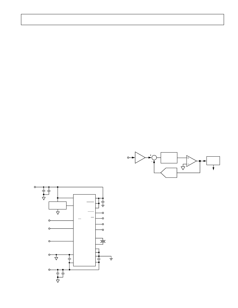
T HE ORY OF OPE RAT ION
T he general block diagram of a sigma-delta ADC is shown in
Figure 8. It contains the following elements.
1. A sample-hold amplifier.
2. A differential amplifier or subtracter.
3. An analog low-pass filter.
4. A 1-bit A/D converter (comparator).
5. A 1-bit DAC.
6. A digital low-pass filter.
In operation, the analog signal sample is fed to the subtracter,
along with the output of the 1-bit DAC. T he filtered difference
signal is fed to the comparator, whose output samples the
difference signal at a frequency many times that of the analog
signal sampling frequency (oversampling).
ANALOG
LOW-PASS
FILTER
COMPARATOR
DIGITAL
FILTER
DIGITAL DATA
S/H AMP
DAC
Figure 8. General Sigma-Delta ADC
Oversampling is fundamental to the operation of sigma-delta
ADCs. Using the quantization noise formula for an ADC:
SNR =
(
6
.02
×
number of bits +
1.76)
dB
a 1-bit ADC or comparator yields an SNR of 7.78 dB.
T he AD7701 samples the input signal at 16 kHz, which spreads
the quantization noise from 0 to 8 kHz. Since the specified
analog input bandwidth of the AD7701 is only 0 to 10 Hz, the
noise energy in this bandwidth would be only 1/800 of the total
quantization noise, even if the noise energy was spread evenly
throughout the spectrum. It is reduced still further by analog
filtering in the modulator loop, which shapes the quantization
noise spectrum to move most of the noise energy to frequencies
above 10 Hz. T he SNR performance in the 0 to 10 Hz range is
conditioned to the 16-bit level in this fashion.
T he output of the comparator provides the digital input for the
1-bit DAC, so that the system functions as a negative feedback
loop that tries to minimize the difference signal. T he digital data
that represents the analog input voltage is contained in the duty
cycle of the pulse train appearing at the output of the compara-
tor. It can be retrieved as a parallel binary data word using a
digital filter.
OFFSE T CALIBRAT ION RANGE
In the system calibration modes (SC2 low) the AD7701
calibrates its offset with respect to the A
IN
pin. T he Offset
Calibration Range specification defines the range of voltages,
expressed as a percentage of V
REF
that the AD7701 can accept
and still calibrate offset accurately.
FULL-SCALE CALIBRAT ION RANGE
T his is the range of voltages that the AD7701 can accept in the
system calibration mode and still calibrate full-scale correctly.
INPUT SPAN
In system calibration schemes, two voltages applied in sequence
to the AD7701’s analog input define the analog input range.
T he input span specification defines the minimum and maxi-
mum input voltages from zero to full-scale that the AD7701 can
accept and still calibrate gain accurately. T he input span is ex-
pressed as a percentage of V
REF.
GE NE RAL DE SCRIPT ION
T he AD7701 is a 16-bit A/D converter with on-chip digital
filtering, intended for the measurement of wide dynamic range,
low frequency signals such as those representing chemical,
physical or biological processes. It contains a charge-balancing
(sigma-delta) ADC, calibration microcontroller with on-chip
static RAM, a clock oscillator and a serial communications port.
T he analog input signal to the AD7701 is continuously sampled
at a rate determined by the frequency of the master clock,
CLK IN. A charge-balancing A/D converter (Sigma-Delta
Modulator) converts the sampled signal into a digital pulse train
whose duty cycle contains the digital information. A six-pole
Gaussian digital low-pass filter processes the output of the
modulator and updates the 16-bit output register at a 4 kHz
rate. T he output data can be read from the serial port randomly
or periodically at any rate up to 4 kHz.
AD7701
MODE
SDATA
SC1
DGND
CLKOUT
CLKIN
AGND
SCLK
SC2
CAL
CS
BP/UP
DV
SS
DV
DD
SLEEP
RANGE
SELECT
CALIBRATE
ANALOG
INPUT
ANALOG
GROUND
–5V
ANALOG
SUPPLY
0.1
μ
F
SERIAL
DATA
SERIAL
CLOCK
READ
(TRANSMIT)
DATA
READY
+5V
ANALOG
SUPPLY
2.5V
0.1
μ
F
0.1
μ
F
VOLTAGE
REFERENCE
DRDY
0.1
μ
F
10
μ
F
AV
DD
V
REF
A
IN
AV
SS
0.1
μ
F
10
μ
F
Figure 7. Typical System Connection Diagram
相關PDF資料 |
PDF描述 |
|---|---|
| AD7701BR | LC2MOS 16-Bit A/D Converter |
| AD7701SQ | LC2MOS 16-Bit A/D Converter |
| AD7701TQ | LC2MOS 16-Bit A/D Converter |
| AD7701 | LC2MOS 16-Bit A/D Converter |
| AD7703 | LC2MOS 20-Bit A/D Converter |
相關代理商/技術參數 |
參數描述 |
|---|---|
| AD7701BR | 制造商:Analog Devices 功能描述:ADC Single Delta-Sigma 4ksps 16-bit Serial 20-Pin SOIC W 制造商:Rochester Electronics LLC 功能描述:16 BIT SIGMA DELTA CONVER - Bulk |
| AD7701BR-REEL | 制造商:Rochester Electronics LLC 功能描述: 制造商:Analog Devices 功能描述: |
| AD7701BRZ | 功能描述:IC ADC 16BIT LC2MOS MONO 20SOIC RoHS:是 類別:集成電路 (IC) >> 數據采集 - 模數轉換器 系列:- 其它有關文件:TSA1204 View All Specifications 標準包裝:1 系列:- 位數:12 采樣率(每秒):20M 數據接口:并聯 轉換器數目:2 功率耗散(最大):155mW 電壓電源:模擬和數字 工作溫度:-40°C ~ 85°C 安裝類型:表面貼裝 封裝/外殼:48-TQFP 供應商設備封裝:48-TQFP(7x7) 包裝:Digi-Reel® 輸入數目和類型:4 個單端,單極;2 個差分,單極 產品目錄頁面:1156 (CN2011-ZH PDF) 其它名稱:497-5435-6 |
| AD7701BRZ-REEL | 功能描述:IC ADC 16BIT LC2MOS 20SOIC RoHS:是 類別:集成電路 (IC) >> 數據采集 - 模數轉換器 系列:- 標準包裝:1 系列:- 位數:14 采樣率(每秒):83k 數據接口:串行,并聯 轉換器數目:1 功率耗散(最大):95mW 電壓電源:雙 ± 工作溫度:0°C ~ 70°C 安裝類型:通孔 封裝/外殼:28-DIP(0.600",15.24mm) 供應商設備封裝:28-PDIP 包裝:管件 輸入數目和類型:1 個單端,雙極 |
| AD7701SQ | 制造商:AD 制造商全稱:Analog Devices 功能描述:LC2MOS 16-Bit A/D Converter |
發布緊急采購,3分鐘左右您將得到回復。