- 您現在的位置:買賣IC網 > PDF目錄373914 > AD7705EB (Analog Devices, Inc.) Precision Zero-Drift Operational Amplifier with Internal Capacitors; Package: SO; No of Pins: 8; Temperature Range: 0°C to +70°C PDF資料下載
參數資料
| 型號: | AD7705EB |
| 廠商: | Analog Devices, Inc. |
| 英文描述: | Precision Zero-Drift Operational Amplifier with Internal Capacitors; Package: SO; No of Pins: 8; Temperature Range: 0°C to +70°C |
| 中文描述: | 3伏/ 5伏1毫瓦2-/3-Channel 16位Σ-Δ模數轉換器(264.12十一) |
| 文件頁數: | 15/32頁 |
| 文件大小: | 264K |
| 代理商: | AD7705EB |
第1頁第2頁第3頁第4頁第5頁第6頁第7頁第8頁第9頁第10頁第11頁第12頁第13頁第14頁當前第15頁第16頁第17頁第18頁第19頁第20頁第21頁第22頁第23頁第24頁第25頁第26頁第27頁第28頁第29頁第30頁第31頁第32頁
AD7705/AD7706
–15–
REV. A
CIRCUIT DESCRIPTION
The AD7705/AD7706 is a sigma-delta A/D converter with on-
chip digital filtering, intended for the measurement of wide
dynamic range, low frequency signals such as those in industrial
control or process control applications. It contains a sigma-delta
(or charge-balancing) ADC, a calibration microcontroller with
on-chip static RAM, a clock oscillator, a digital filter and a bi-
directional serial communications port. The part consumes only
320
μ
A of power supply current, making it ideal for battery-
powered or loop-powered instruments. These parts operate with
a supply voltage of 2.7 V to 3.3 V or 4.75 V to 5.25 V.
The AD7705 contains two programmable-gain fully differential
analog input channels, while the AD7706 contains three pseudo
differential analog input channels. The selectable gains on these
inputs are 1, 2, 4, 8, 16, 32, 64 and 128 allowing the part to
accept unipolar signals of between 0 mV to +20mV and 0 V to
+2.5V, or bipolar signals in the range from
±
20mV to
±
2.5V
when the reference input voltage equals +2.5V. With a refer-
ence voltage of +1.225V, the input ranges are from 0 mV to
+10mV to 0 V to +1.225V in unipolar mode, and from
±
10mV
to
±
1.225 V in bipolar mode. Note that the bipolar ranges are
with respect to AIN(–) on the AD7705, and with respect to
COMMON on the AD7706, and not with respect to GND.
The input signal to the analog input is continuously sampled
at a rate determined by the frequency of the master clock,
MCLKIN, and the selected gain. A charge-balancing A/D
converter (Sigma-Delta Modulator) converts the sampled signal
into a digital pulse train whose duty cycle contains the digital
information. The programmable gain function on the analog
input is also incorporated in this sigma-delta modulator with the
input sampling frequency being modified to give the higher
gains. A sinc
3
digital low-pass filter processes the output of the
sigma-delta modulator and updates the output register at a rate
determined by the first notch frequency of this filter. The out-
put data can be read from the serial port randomly or periodi-
cally at any rate up to the output register update rate. The first
notch of this digital filter (and hence its –3dB frequency) can
be programmed via the Setup Register bits FS0 and FS1. With
a master clock frequency of 2.4576MHz, the programmable
range for this first notch frequency is from 50Hz to 500Hz,
giving a programmable range for the –3dB frequency of
13.1Hz to 131Hz. With a master clock frequency of 1MHz,
the programmable range for this first notch frequency is from
20Hz to 200Hz, giving a programmable range for the –3dB
frequency of 5.24Hz to 52.4Hz.
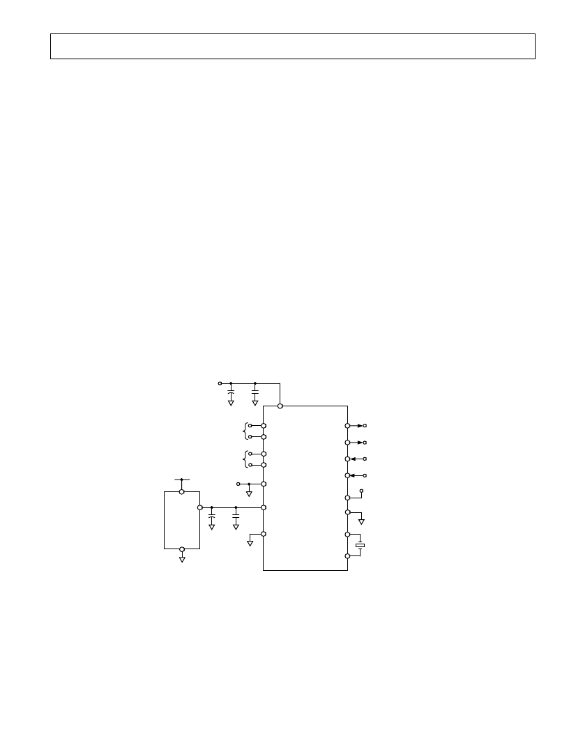
The basic connection diagram for the AD7705 is shown in
Figure 10. This shows the AD7705 being driven from the ana-
log +5V supply. An AD780, precision +2.5 V reference, pro-
vides the reference source for the part. On the digital side, the
part is configured for three-wire operation with
CS
tied to
GND. A quartz crystal or ceramic resonator provide the master
clock source for the part. In most cases, it will be necessary to
connect capacitors on the crystal or resonator to ensure that it
does not oscillate at overtones of its fundamental operating fre-
quency. The values of capacitors will vary, depending on the
manufacturer’s specifications. The same setup applies to the
AD7706.
V
DD
ANALOG
+5V SUPPLY
10
m
F
AIN1(+)
AIN1(–)
AIN2(+)
AIN2(–)
DIFFERENTIAL
ANALOG
INPUT
DIFFERENTIAL
ANALOG
INPUT
GND
REF IN(+)
REF IN(–)
10
m
F
V
IN
ANALOG +5V
SUPPLY
AD780/
REF192
V
OUT
GND
AD7705
DRDY
DATA READY
DOUT
RECEIVE (READ)
DIN
SERIAL DATA
SCLK
SERIAL CLOCK
RESET
+5V
CS
MCLK IN
MCLK OUT
CRYSTAL OR
CERAMIC
RESONATOR
0.1
m
F
0.1
m
F
Figure 10. AD7705 Basic Connection Diagram
相關PDF資料 |
PDF描述 |
|---|---|
| AD7706* | 3 V/5 V. 1 mW 2-/3-Channel 16-Bit. Sigma-Delta ADCs |
| AD7706EB | High Performance Switched Capacitor Universal Filter; Package: PDIP; No of Pins: 14; Temperature Range: 0°C to +70°C |
| AD7706(中文) | 3 V/5 V, 1 Mw 2-/3-Channel 16-Bit, Sigma-Delta ADCs(三輸入通道16位A/D轉換器) |
| AD7705(中文) | 3 V/5 V, 1 Mw 2-/3-Channel 16-Bit, Sigma-Delta ADCs(完全差分輸入通道16位A/D轉換器) |
| AD7707BR | 3 V/5 V, +-10 V Input Range, 1 mW 3-Channel 16-Bit, Sigma-Delta ADC |
相關代理商/技術參數 |
參數描述 |
|---|---|
| AD7706 | 制造商:AD 制造商全稱:Analog Devices 功能描述:3 V/5 V, 1 mW 2-/3-Channel 16-Bit, Sigma-Delta ADCs |
| AD7706BN | 功能描述:IC ADC 16BIT 3CH 16-DIP RoHS:否 類別:集成電路 (IC) >> 數據采集 - 模數轉換器 系列:- 產品培訓模塊:Lead (SnPb) Finish for COTS Obsolescence Mitigation Program 標準包裝:2,500 系列:- 位數:12 采樣率(每秒):3M 數據接口:- 轉換器數目:- 功率耗散(最大):- 電壓電源:- 工作溫度:- 安裝類型:表面貼裝 封裝/外殼:SOT-23-6 供應商設備封裝:SOT-23-6 包裝:帶卷 (TR) 輸入數目和類型:- |
| AD7706BNZ | 功能描述:IC ADC 16BIT 3CHAN 16DIP RoHS:是 類別:集成電路 (IC) >> 數據采集 - 模數轉換器 系列:- 其它有關文件:TSA1204 View All Specifications 標準包裝:1 系列:- 位數:12 采樣率(每秒):20M 數據接口:并聯 轉換器數目:2 功率耗散(最大):155mW 電壓電源:模擬和數字 工作溫度:-40°C ~ 85°C 安裝類型:表面貼裝 封裝/外殼:48-TQFP 供應商設備封裝:48-TQFP(7x7) 包裝:Digi-Reel® 輸入數目和類型:4 個單端,單極;2 個差分,單極 產品目錄頁面:1156 (CN2011-ZH PDF) 其它名稱:497-5435-6 |
| AD7706BNZ1 | 制造商:AD 制造商全稱:Analog Devices 功能描述:3 V/5 V, 1 mW, 2-/3-Channel, 16-Bit, Sigma-Delta ADCs |
發布緊急采購,3分鐘左右您將得到回復。