- 您現在的位置:買賣IC網 > PDF目錄373913 > AD7706BR (ANALOG DEVICES INC) 3 V/5 V, 1 mW 2-/3-Channel 16-Bit, Sigma-Delta ADCs PDF資料下載
參數資料
| 型號: | AD7706BR |
| 廠商: | ANALOG DEVICES INC |
| 元件分類: | ADC |
| 英文描述: | 3 V/5 V, 1 mW 2-/3-Channel 16-Bit, Sigma-Delta ADCs |
| 中文描述: | 3-CH 16-BIT DELTA-SIGMA ADC, SERIAL ACCESS, PDSO16 |
| 封裝: | 0.300 INCH, MS-013AA, SOIC-16 |
| 文件頁數: | 16/32頁 |
| 文件大小: | 264K |
| 代理商: | AD7706BR |
第1頁第2頁第3頁第4頁第5頁第6頁第7頁第8頁第9頁第10頁第11頁第12頁第13頁第14頁第15頁當前第16頁第17頁第18頁第19頁第20頁第21頁第22頁第23頁第24頁第25頁第26頁第27頁第28頁第29頁第30頁第31頁第32頁
AD7705/AD7706
–16–
REV. A
ANALOG INPUT
Analog Input Ranges
The AD7705 contains two differential analog input pairs
AIN1(+), AIN1(–) and AIN2(+), AIN2(–). These input pairs
provide programmable-gain, differential input channels that
can handle either unipolar or bipolar input signals. It should be
noted that the bipolar input signals are referenced to the re-
spective AIN(–) input of each input pair. The AD7706 contains
three pseudo differential analog input pairs AIN1, AIN2 and
AIN3, which are referenced to the COMMON input on the part.
In unbuffered mode, the common-mode range of the input is
from GND to V
DD
, provided that the absolute value of the
analog input voltage lies between GND–30mV and V
DD
+30mV. This means that in unbuffered mode the part can
handle both unipolar and bipolar input ranges for all gains.
Absolute voltages of GND – 200 mV can be accommodated on
the analog inputs at 25
°
C without degradation in performance,
but leakage current increases appreciably with increasing tem-
perature. In buffered mode, the analog inputs can handle
much larger source impedances, but the absolute input voltage
range is restricted to between GND+ 50mV to V
DD
– 1.5 V
which also places restrictions on the common-mode range. This
means that in buffered mode there are some restrictions on the
allowable gains for bipolar input ranges. Care must be taken in
setting up the common-mode voltage and input voltage range
so that the above limits are not exceeded, otherwise there will
be a degradation in linearity performance.
In unbuffered mode, the analog inputs look directly into the
7pF input sampling capacitor, C
SAMP
. The dc input leakage
current in this unbuffered mode is 1nA maximum. As a result,
the analog inputs see a dynamic load that is switched at the
input sample rate (see Figure 11). This sample rate depends on
master clock frequency and selected gain. C
SAMP
is charged to
AIN(+) and discharged to AIN(–) every input sample cycle.
The effective on-resistance of the switch, R
SW
, is typically 7k
.
C
SAMP
must be charged through R
SW
and through any external
source impedances every input sample cycle. Therefore, in
unbuffered mode, source impedances mean a longer charge time
for C
SAMP
and this may result in gain errors on the part. Table
XIV shows the allowable external resistance/capacitance values,
for unbuffered mode, such that no gain error to the 16-bit level
is introduced on the part. Note that these capacitances are
total capacitances on the analog input, external capacitance
plus 10 pF capacitance from the pins and lead frame of the device.
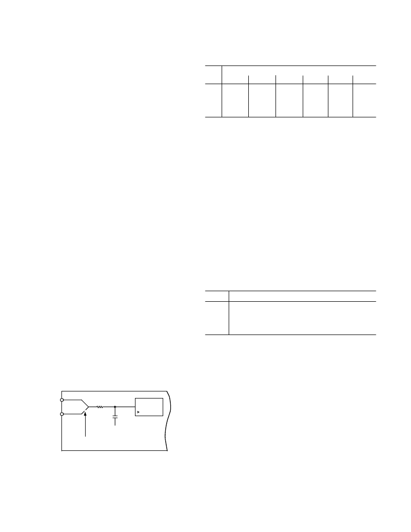
AIN(+)
AIN(–)
SWITCHING FREQUENCY DEPENDS ON
f
CLKIN
AND SELECTED GAIN
R
SW
(7k
V
TYP)
C
(7pF)
HIGH
IMPEDANCE
1G
V
BIAS
Figure 11. Unbuffered Analog Input Structure
Table XIV. External R, C Combination for No 16-Bit Gain
Error (Unbuffered Mode Only)
External Capacitance (pF)
0
50
100
Gain
500
1000
5000
1
2
4
8–128
368 k
177.2 k
82.8 k
35.2 k
90.6 k
44.2 k
21.2 k
9.6 k
54.2 k
26.4 k
12.6 k
5.8 k
14.6 k
7.2 k
3.4 k
1.58
8.2 k
4 k
1.94 k
540
880
2.2 k
1.12 k
240
In buffered mode, the analog inputs look into the high-impedance
inputs stage of the on-chip buffer amplifier. C
SAMP
is charged
via this buffer amplifier such that source impedances do not
affect the charging of C
SAMP
. This buffer amplifier has an offset
leakage current of 1 nA. In this buffered mode, large source
impedances result in a small dc offset voltage developed across
the source impedance, but not in a gain error.
Input Sample Rate
The modulator sample frequency for the AD7705/AD7706
remains at f
CLKIN
/128 (19.2kHz @ f
CLKIN
= 2.4576MHz) re-
gardless of the selected gain. However, gains greater than 1 are
achieved by a combination of multiple input samples per modu-
lator cycle and a scaling of the ratio of reference capacitor to
input capacitor. As a result of the multiple sampling, the input
sample rate of the device varies with the selected gain (see Table
XV). In buffered mode, the input is buffered before the input
sampling capacitor. In unbuffered mode, where the analog
input looks directly into the sampling capacitor, the effective
input impedance is 1/C
SAMP
×
f
S
where C
SAMP
is the input sam-
pling capacitance and f
S
is the input sample rate.
Table XV. Input Sampling Frequency vs. Gain
Gain
Input Sampling Frequency (f
S
)
f
CLKIN
/64 (38.4kHz @ f
CLKIN
= 2.4576MHz)
2
f
CLKIN
/64 (76.8kHz @ f
CLKIN
= 2.4576MHz)
4
×
f
CLKIN
/64 (76.8kHz @ f
CLKIN
= 2.4576MHz)
8
×
f
CLKIN
/64 (307.2kHz @ f
CLKIN
= 2.4576MHz)
1
2
4
8–128
Bipolar/Unipolar Inputs
The analog inputs on the AD7705/AD7706 can accept either
unipolar or bipolar input voltage ranges. Bipolar input ranges do
not imply that the part can handle negative voltages on its analog
input, since the analog input cannot go more negative than
–30 mV to ensure correct operation of these parts. The input
channels are fully differential. As a result, on the AD7705, the
voltage to which the unipolar and bipolar signals on the AIN(+)
input are referenced is the voltage on the respective AIN(–)
input. On the AD7706, the voltages applied to the analog input
channels are referenced to the COMMON input. For example, if
AIN1(–) is +2.5V and the AD7705 is configured for unipolar
operation with a gain of 2 and a V
REF
of +2.5V, the input voltage
range on the AIN1(+) input is +2.5V to +3.75V. If AIN1(–) is
+2.5V and the AD7705 is configured for bipolar mode with a
gain of 2 and a V
REF
of +2.5V, the analog input range on the
AIN1(+) input is +1.25V to +3.75 V (i.e., 2.5V
±
1.25V). If
AIN1(–) is at GND, the part cannot be configured for bipolar
ranges in excess of
±
30mV.
相關PDF資料 |
PDF描述 |
|---|---|
| AD7706BRU | 3 V/5 V, 1 mW 2-/3-Channel 16-Bit, Sigma-Delta ADCs |
| AD7705EB | Precision Zero-Drift Operational Amplifier with Internal Capacitors; Package: SO; No of Pins: 8; Temperature Range: 0°C to +70°C |
| AD7706* | 3 V/5 V. 1 mW 2-/3-Channel 16-Bit. Sigma-Delta ADCs |
| AD7706EB | High Performance Switched Capacitor Universal Filter; Package: PDIP; No of Pins: 14; Temperature Range: 0°C to +70°C |
| AD7706(中文) | 3 V/5 V, 1 Mw 2-/3-Channel 16-Bit, Sigma-Delta ADCs(三輸入通道16位A/D轉換器) |
相關代理商/技術參數 |
參數描述 |
|---|---|
| AD7706BR-REEL | 制造商:Analog Devices 功能描述:ADC Single Delta-Sigma 500sps 16-bit Serial 16-Pin SOIC W T/R |
| AD7706BR-REEL7 | 功能描述:IC ADC 16BIT 3CH 16-SOIC T/R RoHS:否 類別:集成電路 (IC) >> 數據采集 - 模數轉換器 系列:- 標準包裝:1,000 系列:- 位數:16 采樣率(每秒):45k 數據接口:串行 轉換器數目:2 功率耗散(最大):315mW 電壓電源:模擬和數字 工作溫度:0°C ~ 70°C 安裝類型:表面貼裝 封裝/外殼:28-SOIC(0.295",7.50mm 寬) 供應商設備封裝:28-SOIC W 包裝:帶卷 (TR) 輸入數目和類型:2 個單端,單極 |
| AD7706BRU | 功能描述:IC ADC 16BIT 3CH 16-TSSOP RoHS:否 類別:集成電路 (IC) >> 數據采集 - 模數轉換器 系列:- 標準包裝:1,000 系列:- 位數:12 采樣率(每秒):300k 數據接口:并聯 轉換器數目:1 功率耗散(最大):75mW 電壓電源:單電源 工作溫度:0°C ~ 70°C 安裝類型:表面貼裝 封裝/外殼:24-SOIC(0.295",7.50mm 寬) 供應商設備封裝:24-SOIC 包裝:帶卷 (TR) 輸入數目和類型:1 個單端,單極;1 個單端,雙極 |
| AD7706BRU-REEL | 制造商:Analog Devices 功能描述:ADC Single Delta-Sigma 500sps 16-bit Serial 16-Pin TSSOP T/R 制造商:Analog Devices 功能描述:ADC SGL DELTA-SIGMA 0.5KSPS 16BIT SERL 16TSSOP - Tape and Reel 制造商:Rochester Electronics LLC 功能描述:LOW COST 3CHNL 16-6 SIGMA DELTA ADC I.C. - Tape and Reel |
| AD7706BRU-REEL7 | 功能描述:IC ADC 16BIT 3CH 16-TSSOP T/R RoHS:否 類別:集成電路 (IC) >> 數據采集 - 模數轉換器 系列:- 標準包裝:1,000 系列:- 位數:16 采樣率(每秒):45k 數據接口:串行 轉換器數目:2 功率耗散(最大):315mW 電壓電源:模擬和數字 工作溫度:0°C ~ 70°C 安裝類型:表面貼裝 封裝/外殼:28-SOIC(0.295",7.50mm 寬) 供應商設備封裝:28-SOIC W 包裝:帶卷 (TR) 輸入數目和類型:2 個單端,單極 |
發布緊急采購,3分鐘左右您將得到回復。