- 您現在的位置:買賣IC網 > PDF目錄373914 > AD7712SQ (ANALOG DEVICES INC) LC2MOS Signal Conditioning ADC PDF資料下載
參數資料
| 型號: | AD7712SQ |
| 廠商: | ANALOG DEVICES INC |
| 元件分類: | ADC |
| 英文描述: | LC2MOS Signal Conditioning ADC |
| 中文描述: | 2-CH 24-BIT DELTA-SIGMA ADC, SERIAL ACCESS, CDIP24 |
| 封裝: | 0.300 INCH, HERMETIC SEALED, CERDIP-24 |
| 文件頁數: | 21/28頁 |
| 文件大小: | 229K |
| 代理商: | AD7712SQ |
第1頁第2頁第3頁第4頁第5頁第6頁第7頁第8頁第9頁第10頁第11頁第12頁第13頁第14頁第15頁第16頁第17頁第18頁第19頁第20頁當前第21頁第22頁第23頁第24頁第25頁第26頁第27頁第28頁
2
–21–
REV. E
AD7712
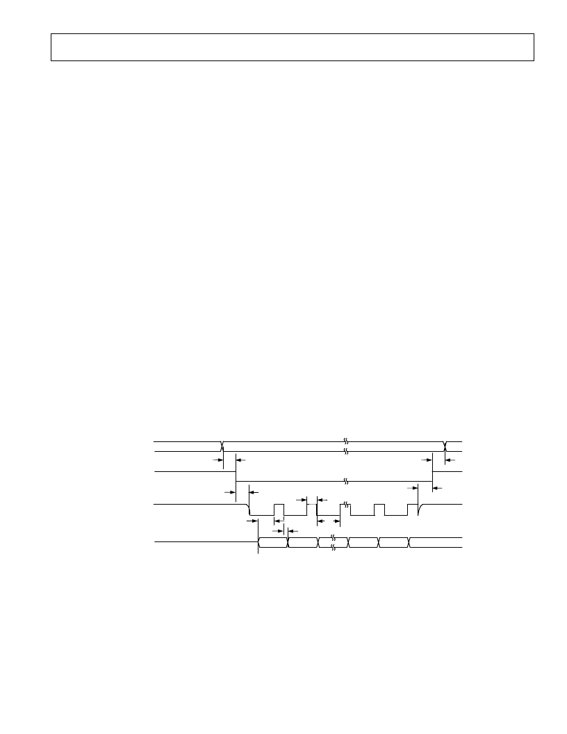
Write Operation
Data can be written to either the control register or calibration
registers. In either case, the write operation is not affected by
the
DRDY
line and the write operation does not have any effect
on the status of
DRDY
. A write operation to the control register
or the calibration register must always write 24 bits to the
respective register.
Figure 12 shows a write operation to the AD7712. A0 deter-
mines whether a write operation transfers data to the control
register or to the calibration registers. This A0 signal must remain
valid for the duration of the serial write operation. The falling
edge of
TFS
enables the internally generated SCLK output.
The serial data to be loaded to the AD7712 must be valid on
the rising edge of this SCLK signal. Data is clocked into the
AD7712 on the rising edge of the SCLK signal with the MSB
transferred first. On the last active high time of SCLK, the LSB
is loaded to the AD7712. Subsequent to the next falling edge of
SCLK, the SCLK output is turned off. (The timing diagram of
Figure 12 assumes a pull-up resistor on the SCLK line.)
External Clocking Mode
The AD7712 is configured for its external clocking mode by
tying the MODE pin low. In this mode, SCLK of the AD7712
is configured as an input, and an external serial clock must be
provided to this SCLK pin. This external clocking mode is
designed for direct interface to systems which provide a serial
clock output which is synchronized to the serial data output,
including microcontrollers such as the 80C51, 87C51, 68HC11
and 68HC05 and most digital signal processors.
Read Operation
As with the self-clocking mode, data can be read from either the
output register, the control register or the calibration registers.
A0 determines whether the data read accesses data from the
control register or from the output/calibration registers. This A0
signal must remain valid for the duration of the serial read
operation. With A0 high, data is accessed from either the output
register or from the calibration registers. With A0 low, data is
accessed from the control register.
The function of the
DRDY
line is dependent only on the output
update rate of the device and the reading of the output data
register.
DRDY
goes low when a new data word is available in
the output data register. It is reset high when the last bit of data
(either 16th bit or 24th bit) is read from the output register. If
data is not read from the output register, the
DRDY
line will
remain low. The output register will continue to be updated at
the output update rate, but
DRDY
will not indicate this. A read
from the device in this circumstance will access the most recent
word in the output register. If a new data word becomes avail-
able to the output register while data is being read from the
output register,
DRDY
will not indicate this and the new data
word will be lost to the user.
DRDY
is not affected by reading
from the control register or the calibration register.
Data can only be accessed from the output data register when
DRDY
is low. If
RFS
goes low while
DRDY
is high, no data
transfer will take place.
DRDY
does not have any effect on reading
data from the control register or from the calibration registers.
Figures 13a and 13b show timing diagrams for reading from the
AD7712 in the external clocking mode. Figure 13a shows a
situation where all the data is read from the AD7712 in one read
operation. Figure 13b shows a situation where the data is read
from the AD7712 over a number of read operations. Both read
operations show a read from the AD7712’s output data register.
A read from the control register or calibration registers is similar,
but in these cases the
DRDY
line is not related to the read func-
tion. Depending on the output update rate, it can go low at any
stage in the control/calibration register read cycle without affect-
ing the read and its status should be ignored. A read operation
from either the control or calibration registers must always read
24 bits of data from the respective register.
SDATA (O)
SCLK (O)
TFS
(I)
A0 (I)
MSB
LSB
t
15
t
16
t
17
t
18
t
19
t
14
t
9
t
10
Figure 12. Self-Clocking Mode, Control/Calibration Register Write Operation
相關PDF資料 |
PDF描述 |
|---|---|
| AD7712* | Rail-to-Rail, Very Low Noise Universal Dual Filter Building Block; Package: SSOP; No of Pins: 16; Temperature Range: 0°C to +70°C |
| AD7712 | Signal Conditioning ADC(LC2MOS信號調節A/D轉換器) |
| AD7713* | LC2MOS Loop-Powered Signal Conditioning ADC |
| AD7713AN | LC2MOS Loop-Powered Signal Conditioning ADC |
| AD7713AQ | LC2MOS Loop-Powered Signal Conditioning ADC |
相關代理商/技術參數 |
參數描述 |
|---|---|
| AD7713 | 制造商:AD 制造商全稱:Analog Devices 功能描述:LC2MOS Loop-Powered Signal Conditioning ADC |
| AD7713AN | 功能描述:IC ADC 24BIT SIGMA-DELTA 24-DIP RoHS:否 類別:集成電路 (IC) >> 數據采集 - 模數轉換器 系列:- 產品培訓模塊:Lead (SnPb) Finish for COTS Obsolescence Mitigation Program 標準包裝:2,500 系列:- 位數:12 采樣率(每秒):3M 數據接口:- 轉換器數目:- 功率耗散(最大):- 電壓電源:- 工作溫度:- 安裝類型:表面貼裝 封裝/外殼:SOT-23-6 供應商設備封裝:SOT-23-6 包裝:帶卷 (TR) 輸入數目和類型:- |
| AD7713ANZ | 功能描述:IC ADC 24BIT SIGMA-DELTA 24-DIP RoHS:是 類別:集成電路 (IC) >> 數據采集 - 模數轉換器 系列:- 其它有關文件:TSA1204 View All Specifications 標準包裝:1 系列:- 位數:12 采樣率(每秒):20M 數據接口:并聯 轉換器數目:2 功率耗散(最大):155mW 電壓電源:模擬和數字 工作溫度:-40°C ~ 85°C 安裝類型:表面貼裝 封裝/外殼:48-TQFP 供應商設備封裝:48-TQFP(7x7) 包裝:Digi-Reel® 輸入數目和類型:4 個單端,單極;2 個差分,單極 產品目錄頁面:1156 (CN2011-ZH PDF) 其它名稱:497-5435-6 |
| AD7713AQ | 制造商:Rochester Electronics LLC 功能描述:24 BIT SIGMA DELTA ADC IC - Bulk |
發布緊急采購,3分鐘左右您將得到回復。