- 您現(xiàn)在的位置:買賣IC網(wǎng) > PDF目錄373914 > AD7713 (Analog Devices, Inc.) Loop-Powered Signal Conditioning ADC(循環(huán)驅(qū)動LC2MOS信號調(diào)節(jié)A/D轉(zhuǎn)換器) PDF資料下載
參數(shù)資料
| 型號: | AD7713 |
| 廠商: | Analog Devices, Inc. |
| 英文描述: | Loop-Powered Signal Conditioning ADC(循環(huán)驅(qū)動LC2MOS信號調(diào)節(jié)A/D轉(zhuǎn)換器) |
| 中文描述: | 回路供電信號調(diào)理模數(shù)轉(zhuǎn)換器(循環(huán)驅(qū)動LC2MOS信號調(diào)節(jié)的A / D轉(zhuǎn)換器) |
| 文件頁數(shù): | 7/28頁 |
| 文件大小: | 529K |
| 代理商: | AD7713 |
第1頁第2頁第3頁第4頁第5頁第6頁當(dāng)前第7頁第8頁第9頁第10頁第11頁第12頁第13頁第14頁第15頁第16頁第17頁第18頁第19頁第20頁第21頁第22頁第23頁第24頁第25頁第26頁第27頁第28頁
2
–7–
REV. C
AD7713
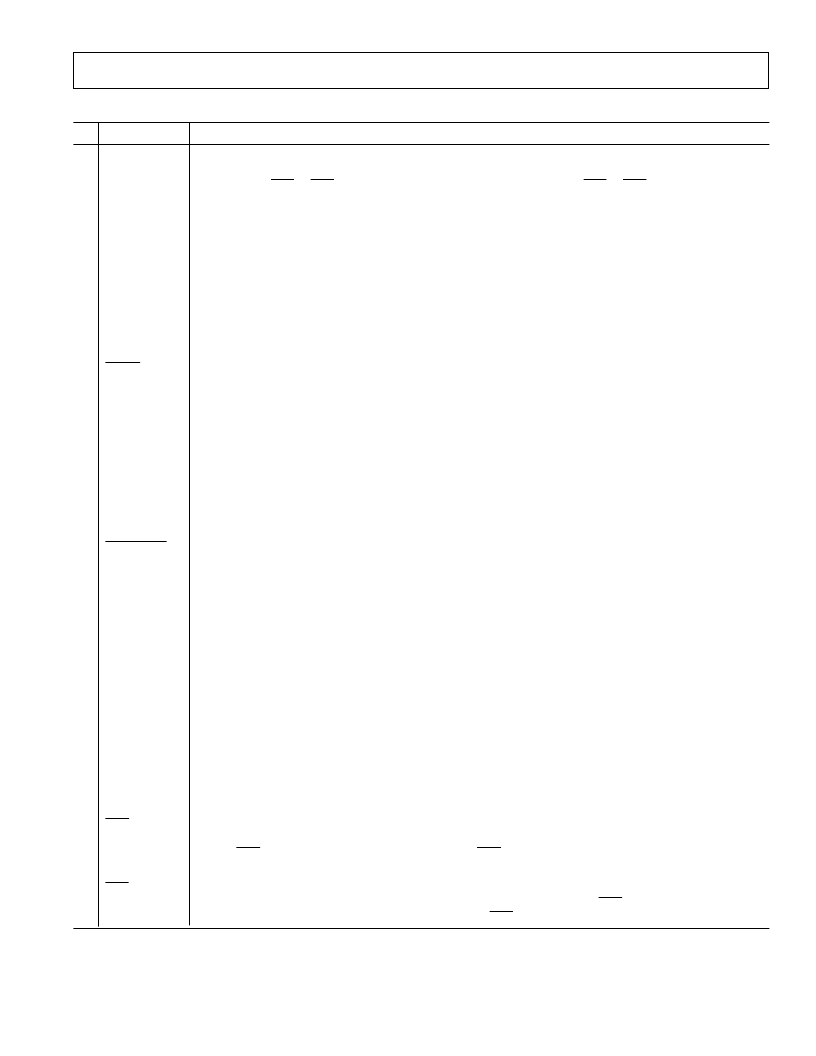
PIN FUNCTION DESCRIPTION
Pin
Mnemonic
Function
1
SCLK
Serial Clock. Logic input/output depending on the status of the MODE pin. When MODE is high, the
device is in its self-clocking mode and the SCLK pin provides a serial clock output. This SCLK becomes
active when
RFS
or
TFS
goes low and it goes high impedance when either
RFS
or
TFS
returns high or when
the device has completed transmission of an output word. When MODE is low, the device is in its external
clocking mode and the SCLK pin acts as an input. This input serial clock can be a continuous clock with all
data transmitted in a continuous train of pulses. Alternatively, it can be a noncontinuous clock with the
information being transmitted to the AD7713 in smaller batches of data.
Master Clock signal for the device. This can be provided in the form of a crystal or external clock. A crystal can
be tied across the MCLK IN and MCLK OUT pins. Alternatively, the MCLK IN pin can be driven with a
CMOS-compatible clock and MCLK OUT left unconnected. The clock input frequency is nominally 2 MHz.
When the master clock for the device is a crystal, the crystal is connected between MCLK IN and MCLK OUT.
Address Input. With this input low, reading and writing to the device is to the control register. With this nput
high, access is to either the data register or the calibration registers.
Logic Input which allows for synchronization of the digital filters when using a number of AD7713s. It resets
the nodes of the digital filter.
Logic Input. When this pin is high, the device is in its self-clocking mode; with this pin low, the device is in its
external clocking mode.
Analog Input Channel 1. Positive input of the programmable gain differential analog input. The AIN1(+) input
is connected to an output current source which can be used to check that an external transducer has burnt out
or gone open circuit. This output current source can be turned on/off via the control register.
Analog Input Channel 1. Negative input of the programmable gain differential analog input.
Analog Input Channel 2. Positive input of the programmable gain differential analog input.
Analog Input Channel 2. Negative input of the programmable gain differential analog input.
Logic Input. Taking this pin low shuts down the internal analog and digital circuitry, reducing power
consumption to less than 50
μ
W.
Analog Positive Supply Voltage, +5 V to +10 V.
Constant Current Output. A nominal 200
μ
A constant current is provided at this pin and this can be used
as the excitation current for RTDs. This, current can be turned on or off via the control register.
Reference Input. The REF IN(–) can lie anywhere between AV
DD
and AGND provided REF IN(+) is
greater than REF IN(–).
Reference Input. The reference input is differential providing that REF IN(+) is greater than REF IN(–).
REF IN(+) can lie anywhere between AV
DD
and AGND.
Constant Current Output. A nominal 200
μ
A constant current is provided at this pin and this can be used
as the excitation current for RTDs. This, current can be turned on or off via the control register. This
second current can be used to eliminate lead resistanced errors in three-wire RTD configurations.
Analog Input Channel 3. High level analog input which accepts an analog input voltage range of
4
×
V
REF
/GAIN. At the nominal V
REF
of +2.5 V and a gain of 1, the AIN3 input voltage range is
0 to
±
10 V.
Ground Reference Point for Analog Circuitry.
Transmit Frame Synchronization. Active low logic input used to write serial data to the device with serial
data expected after the falling edge of this pulse. In the self-clocking mode, the serial clock becomes active
after
TFS
goes low. In the external clocking mode,
TFS
must go low before the first bit of the data word
is written to the part.
Receive Frame Synchronization. Active low logic input used to access serial data from the device. In the
self-clocking mode, the SCLK and SDATA lines both become active after
RFS
goes low. In the external
clocking mode, the SDATA line becomes active after
RFS
goes low.
2
MCLK IN
3
4
MCLK OUT
A0
5
SYNC
6
MODE
7
AIN1(+)
8
9
AIN1(–)
AIN2(+)
AIN2(–)
STANDBY
10
11
12
13
AV
DD
RTD1
14
REF IN(–)
15
REF IN(+)
16
RTD2
17
AIN3
18
19
AGND
TFS
20
RFS
相關(guān)PDF資料 |
PDF描述 |
|---|---|
| AD7714AN-3 | VARISTOR 30VRMS 0805 SMD |
| AD7714AN-5 | VARISTOR 40VRMS 1206 SMD |
| AD7714YRU | 3 V/5 V, CMOS, 500 uA Signal Conditioning ADC |
| AD7714* | 3 V/5 V. CMOS. 500 uA Signal Conditioning ADC |
| AD7714ARS-3 | 3 V/5 V, CMOS, 500 uA Signal Conditioning ADC |
相關(guān)代理商/技術(shù)參數(shù) |
參數(shù)描述 |
|---|---|
| AD7713AN | 功能描述:IC ADC 24BIT SIGMA-DELTA 24-DIP RoHS:否 類別:集成電路 (IC) >> 數(shù)據(jù)采集 - 模數(shù)轉(zhuǎn)換器 系列:- 產(chǎn)品培訓(xùn)模塊:Lead (SnPb) Finish for COTS Obsolescence Mitigation Program 標(biāo)準(zhǔn)包裝:2,500 系列:- 位數(shù):12 采樣率(每秒):3M 數(shù)據(jù)接口:- 轉(zhuǎn)換器數(shù)目:- 功率耗散(最大):- 電壓電源:- 工作溫度:- 安裝類型:表面貼裝 封裝/外殼:SOT-23-6 供應(yīng)商設(shè)備封裝:SOT-23-6 包裝:帶卷 (TR) 輸入數(shù)目和類型:- |
| AD7713ANZ | 功能描述:IC ADC 24BIT SIGMA-DELTA 24-DIP RoHS:是 類別:集成電路 (IC) >> 數(shù)據(jù)采集 - 模數(shù)轉(zhuǎn)換器 系列:- 其它有關(guān)文件:TSA1204 View All Specifications 標(biāo)準(zhǔn)包裝:1 系列:- 位數(shù):12 采樣率(每秒):20M 數(shù)據(jù)接口:并聯(lián) 轉(zhuǎn)換器數(shù)目:2 功率耗散(最大):155mW 電壓電源:模擬和數(shù)字 工作溫度:-40°C ~ 85°C 安裝類型:表面貼裝 封裝/外殼:48-TQFP 供應(yīng)商設(shè)備封裝:48-TQFP(7x7) 包裝:Digi-Reel® 輸入數(shù)目和類型:4 個單端,單極;2 個差分,單極 產(chǎn)品目錄頁面:1156 (CN2011-ZH PDF) 其它名稱:497-5435-6 |
| AD7713AQ | 制造商:Rochester Electronics LLC 功能描述:24 BIT SIGMA DELTA ADC IC - Bulk |
| AD7713AR | 功能描述:IC ADC SIGNAL COND LC2MOS 24SOIC RoHS:否 類別:集成電路 (IC) >> 數(shù)據(jù)采集 - 模數(shù)轉(zhuǎn)換器 系列:- 產(chǎn)品培訓(xùn)模塊:Lead (SnPb) Finish for COTS Obsolescence Mitigation Program 標(biāo)準(zhǔn)包裝:2,500 系列:- 位數(shù):12 采樣率(每秒):3M 數(shù)據(jù)接口:- 轉(zhuǎn)換器數(shù)目:- 功率耗散(最大):- 電壓電源:- 工作溫度:- 安裝類型:表面貼裝 封裝/外殼:SOT-23-6 供應(yīng)商設(shè)備封裝:SOT-23-6 包裝:帶卷 (TR) 輸入數(shù)目和類型:- |
發(fā)布緊急采購,3分鐘左右您將得到回復(fù)。