- 您現在的位置:買賣IC網 > PDF目錄373914 > AD7713AN (ANALOG DEVICES INC) LC2MOS Loop-Powered Signal Conditioning ADC PDF資料下載
參數資料
| 型號: | AD7713AN |
| 廠商: | ANALOG DEVICES INC |
| 元件分類: | ADC |
| 英文描述: | LC2MOS Loop-Powered Signal Conditioning ADC |
| 中文描述: | 3-CH 24-BIT DELTA-SIGMA ADC, SERIAL ACCESS, PDIP24 |
| 封裝: | 0.300 INCH, PLASTIC, DIP-24 |
| 文件頁數: | 13/28頁 |
| 文件大小: | 516K |
| 代理商: | AD7713AN |
第1頁第2頁第3頁第4頁第5頁第6頁第7頁第8頁第9頁第10頁第11頁第12頁當前第13頁第14頁第15頁第16頁第17頁第18頁第19頁第20頁第21頁第22頁第23頁第24頁第25頁第26頁第27頁第28頁
2
–13–
REV. C
AD7713
The AD7713 gives the user access to the on-chip calibration
registers allowing the microprocessor to read the device’s cali-
bration coefficients and also to write its own calibration coeffi-
cients to the part from prestored values in E
2
PROM. This gives
the microprocessor much greater control over the AD7713’s
calibration procedure. It also means that the user can verify that
the device has performed its calibration correctly by comparing the
coefficients after calibration with prestored values in E
2
PROM.
For battery operation or low power systems, the AD7713 offers
a standby mode (controlled by the
STANDBY
pin) that reduces
idle power consumption to typically 150
μ
W.
THEORY OF OPERATION
The general block diagram of a sigma-delta ADC is shown in
Figure 4. It contains the following elements:
1. A sample-hold amplifier.
2. A differential amplifier or subtracter.
3. An analog low-pass filter.
4. A 1-bit A/D converter (comparator).
5. A 1-bit DAC.
6. A digital low-pass filter.
S/H AMP
ANALOG
LOW-PASS
FILTER
DAC
COMPARATOR
DIGITAL
FILTER
DIGITAL DATA
Figure 4. General Sigma-Delta ADC
In operation, the analog signal sample is fed to the subtracter,
along with the output of the 1-bit DAC. The filtered difference
signal is fed to the comparator, whose output samples the differ-
ence signal at a frequency many times that of the analog signal
sampling frequency (oversampling).
Oversampling is fundamental to the operation of sigma-delta
ADCs. Using the quantization noise formula for an ADC:
SNR = (
6.02
×
number of bits +
1.76)
dB,
a 1-bit ADC or comparator yields an SNR of 7.78 dB.
The AD7713 samples the input signal at a frequency of 7.8 kHz or
greater (see Table III). As a result, the quantization noise is
spread over a much wider frequency than that of the band of
interest. The noise in the band of interest is reduced still further
by analog filtering in the modulator loop, which shapes the
quantization noise spectrum to move most of the noise energy to
frequencies outside the bandwidth of interest. The noise perfor-
mance is thus improved from this 1-bit level to the performance
outlined in Tables I and II and in Figure 2.
The output of the comparator provides the digital input for the
1-bit DAC, so that the system functions as a negative feedback
loop that tries to minimize the difference signal. The digital data
that represents the analog input voltage is contained in the duty
cycle of the pulse train appearing at the output of the compara-
tor. It can be retrieved as a parallel binary data word using a
digital filter.
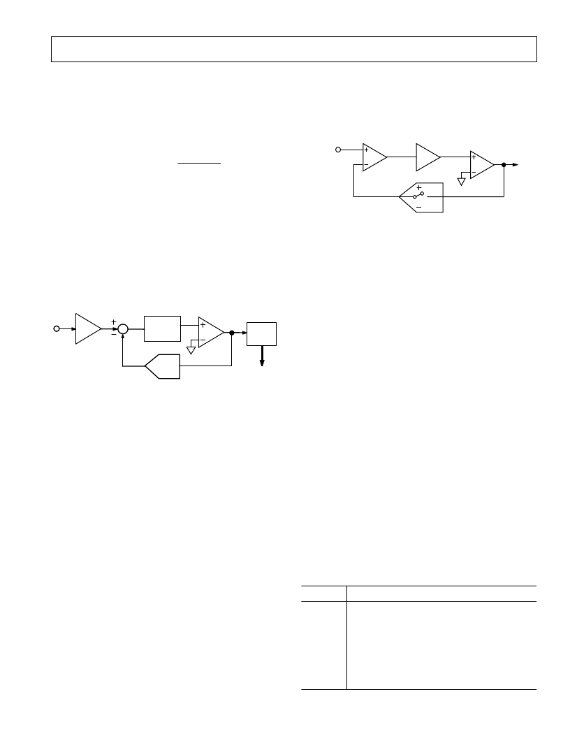
Sigma-delta ADCs are generally described by the order of the
analog low-pass filter. A simple example of a first order sigma-
delta ADC is shown in Figure 5. This contains only a first order
low-pass filter or integrator. It also illustrates the derivation of
the alternative name for these devices: Charge Balancing ADCs
WIN
FS
COMPARATOR
DIFFERENTIAL
AMPLIFIER
INTEGRATOR
∫
FS
DAC
Figure 5. Basic Charge-Balancing ADC
It consists of a differential amplifier (whose output is the differ-
ence between the analog input and the output of a 1-bit DAC),
an integrator and a comparator. The term charge balancing,
comes from the fact that this system is a negative feedback loop
that tries to keep the net charge on the integrator capacitor at
zero by balancing charge injected by the input voltage with
charge injected by the 1-bit DAC. When the analog input is
zero, the only contribution to the integrator output comes from
the 1-bit DAC. For the net charge on the integrator capacitor to
be zero, the DAC output must spend half its time at +FS and
half its time at –FS. Assuming ideal components, the duty cycle
of the comparator will be 50%.
When a positive analog input is applied, the output of the 1-bit
DAC must spend a larger proportion of the time at +FS, so the
duty cycle of the comparator increases. When a negative input
voltage is applied, the duty cycle decreases.
The AD7713 uses a second-order sigma-delta modulator and a
digital filter that provides a rolling average of the sampled out-
put. After power-up or if there is a step change in the input
voltage, there is a settling time that must elapse before valid
data is obtained.
Input Sample Rate
The modulator sample frequency for the device remains at
f
CLK IN
/512 (3.9 kHz @ f
CLK IN
= 2 MHz) regardless of the
selected gain. However, gains greater than
×
1 are achieved by a
combination of multiple input samples per modulator cycle and
a scaling of the ratio of reference capacitor to input capacitor.
As a result of the multiple sampling, the input sample rate of
the device varies with the selected gain (see Table III). The ef-
fective input impedance is 1/C
×
f
S
where C is the input sam-
pling capacitance and f
S
is the input sample rate.
Table III. Input Sampling Frequency vs. Gain
Gain
Input Sampling Frequency (f
S
)
1
2
4
8
16
32
64
128
f
CLK IN
/256 (7.8 kHz @ f
CLK IN
= 2 MHz)
2
f
CLK IN
/256 (15.6 kHz @ f
CLK IN
= 2 MHz)
4
×
f
CLK IN
/256 (31.2 kHz @ f
CLK IN
= 2 MHz)
8
×
f
CLK IN
/256 (62.4 kHz @ f
CLK IN
= 2 MHz)
8
×
f
CLK IN
/256 (62.4 kHz @ f
CLK IN
= 2 MHz)
8
×
f
CLK IN
/256 (62.4 kHz @ f
CLK IN
= 2 MHz)
8
×
f
CLK IN
/256 (62.4 kHz @ f
CLK IN
= 2 MHz)
8
×
f
CLK IN
/256 (62.4 kHz @ f
CLK IN
= 2 MHz)
相關PDF資料 |
PDF描述 |
|---|---|
| AD7713AQ | LC2MOS Loop-Powered Signal Conditioning ADC |
| AD7713AR | LC2MOS Loop-Powered Signal Conditioning ADC |
| AD7713SQ | LC2MOS Loop-Powered Signal Conditioning ADC |
| AD7713 | Loop-Powered Signal Conditioning ADC(循環驅動LC2MOS信號調節A/D轉換器) |
| AD7714AN-3 | VARISTOR 30VRMS 0805 SMD |
相關代理商/技術參數 |
參數描述 |
|---|---|
| AD7713ANZ | 功能描述:IC ADC 24BIT SIGMA-DELTA 24-DIP RoHS:是 類別:集成電路 (IC) >> 數據采集 - 模數轉換器 系列:- 其它有關文件:TSA1204 View All Specifications 標準包裝:1 系列:- 位數:12 采樣率(每秒):20M 數據接口:并聯 轉換器數目:2 功率耗散(最大):155mW 電壓電源:模擬和數字 工作溫度:-40°C ~ 85°C 安裝類型:表面貼裝 封裝/外殼:48-TQFP 供應商設備封裝:48-TQFP(7x7) 包裝:Digi-Reel® 輸入數目和類型:4 個單端,單極;2 個差分,單極 產品目錄頁面:1156 (CN2011-ZH PDF) 其它名稱:497-5435-6 |
| AD7713AQ | 制造商:Rochester Electronics LLC 功能描述:24 BIT SIGMA DELTA ADC IC - Bulk |
| AD7713AR | 功能描述:IC ADC SIGNAL COND LC2MOS 24SOIC RoHS:否 類別:集成電路 (IC) >> 數據采集 - 模數轉換器 系列:- 產品培訓模塊:Lead (SnPb) Finish for COTS Obsolescence Mitigation Program 標準包裝:2,500 系列:- 位數:12 采樣率(每秒):3M 數據接口:- 轉換器數目:- 功率耗散(最大):- 電壓電源:- 工作溫度:- 安裝類型:表面貼裝 封裝/外殼:SOT-23-6 供應商設備封裝:SOT-23-6 包裝:帶卷 (TR) 輸入數目和類型:- |
| AD7713AR-REEL | 制造商:Analog Devices 功能描述:24-BIT SIGMA DELTA ADC IC - Tape and Reel |
| AD7713AR-REEL7 | 制造商:AD 制造商全稱:Analog Devices 功能描述:LC2MOS Loop-Powered Signal Conditioning ADC |
發布緊急采購,3分鐘左右您將得到回復。