- 您現(xiàn)在的位置:買賣IC網(wǎng) > PDF目錄373914 > AD7715AN-3 (ANALOG DEVICES INC) 3 V/5 V, 450 uA 16-Bit, Sigma-Delta ADC PDF資料下載
參數(shù)資料
| 型號: | AD7715AN-3 |
| 廠商: | ANALOG DEVICES INC |
| 元件分類: | ADC |
| 英文描述: | 3 V/5 V, 450 uA 16-Bit, Sigma-Delta ADC |
| 中文描述: | 1-CH 16-BIT DELTA-SIGMA ADC, SERIAL ACCESS, PDIP16 |
| 封裝: | 0.300 INCH, PLASTIC, MS-001AB, DIP-16 |
| 文件頁數(shù): | 21/31頁 |
| 文件大小: | 474K |
| 代理商: | AD7715AN-3 |
第1頁第2頁第3頁第4頁第5頁第6頁第7頁第8頁第9頁第10頁第11頁第12頁第13頁第14頁第15頁第16頁第17頁第18頁第19頁第20頁當前第21頁第22頁第23頁第24頁第25頁第26頁第27頁第28頁第29頁第30頁第31頁
AD7715
–21–
REV. C
Measurement errors due to offset drift or gain drift can be elimi-
nated at any time by recalibrating the converter. Using the sys-
tem calibration mode can also minimize offset and gain errors in
the signal conditioning circuitry. Integral and differential linear-
ity errors are not significantly affected by temperature changes.
POWER SUPPLIES
There is no specific power sequence required for the AD7715;
either the AV
DD
or the DV
DD
supply can come up first. While
the latch-up performance of the AD7715 is good, it is important
that power is applied to the AD7715 before signals at REFIN,
AIN or the logic input pins in order to avoid excessive currents.
If this is not possible, then the current which flows in any of
these pins should be limited. If separate supplies are used for
the AD7715 and the system digital circuitry, then the AD7715
should be powered up first. If it is not possible to guarantee
this, then current limiting resistors should be placed in series
with the logic inputs to again limit the current.
During normal operation the AD7715 analog supply (AV
DD
)
should always be greater than or equal to its digital supply (DV
DD
).
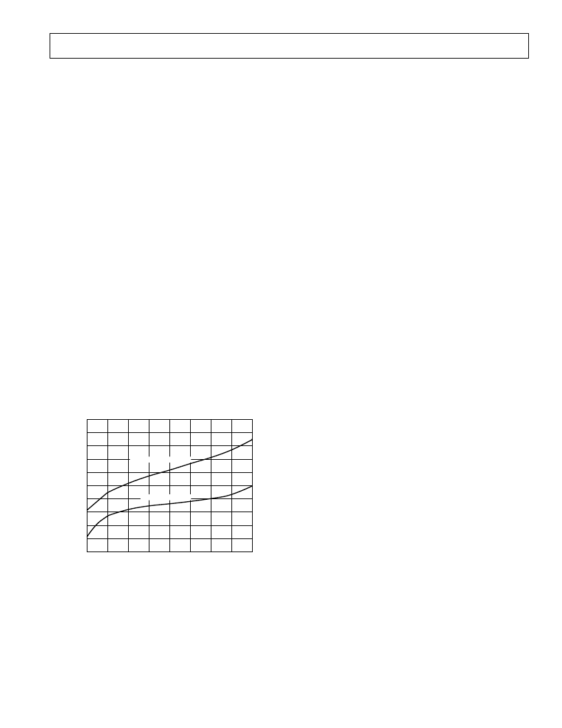
Supply Current
The current consumption on the AD7715 is specified for sup-
plies in the range +3V to +3.6V and in the range +4.75V to
+5.25V. The part operates over a +2.85V to +5.25V supply
range and the I
DD
for the part varies as the supply voltage varies
over this range. Figure 5 shows the variation of the typical
I
DD
with V
DD
voltage for both a 1 MHz external clock and a
2.4576 MHz external clock at +25
°
C. The AD7715 is operated
in unbuffered mode. The relationship shows that the I
DD
is
minimized by operating the part with lower V
DD
voltages. I
DD
on the AD7715 is also minimized by using an external master
clock or by optimizing external components when using the on-
chip oscillator circuit.
SUPPLY VOLTAGE (AV
DD
& DV
DD
) – Volts
0
2.85
0.9
1.0
0.8
0.7
0.6
0.5
0.4
0.3
0.2
0.1
3.15
3.45
4.05
4.35
4.65
4.95
5.25
3.75
MCLK IN = 2.4576MHz
MCLK IN = 1MHz
S
D
D
)
Figure 5. I
DD
vs. Supply Voltage
Grounding and Layout
Since the analog inputs and reference input are differential,
most of the voltages in the analog modulator are common-mode
voltages. The excellent common-mode rejection of the part will
remove common-mode noise on these inputs. The analog and
digital supplies to the AD7715 are independent and separately
pinned out to minimize coupling between the analog and digital
sections of the device. The digital filter will provide rejection of
broadband noise on the power supplies, except at integer mul-
tiples of the modulator sampling frequency. The digital filter
also removes noise from the analog and reference inputs pro-
vided those noise sources do not saturate the analog modulator.
As a result, the AD7715 is more immune to noise interference
that a conventional high resolution converter. However, because
the resolution of the AD7715 is so high and the noise levels
from the AD7715 so low, care must be taken with regard to
grounding and layout.
The printed circuit board which houses the AD7715 should be
designed such that the analog and digital sections are separated
and confined to certain areas of the board. This facilitates the
use of ground planes which can be separated easily. A minimum
etch technique is generally best for ground planes as it gives the
best shielding. Digital and analog ground planes should only be
joined in one place. If the AD7715 is the only device requiring
an AGND to DGND connection, then the ground planes
should be connected at the AGND and DGND pins of the
AD7715. If the AD7715 is in a system where multiple devices
require AGND to DGND connections, the connection should
still be made at one point only, a star ground point which
should be established as close as possible to the AD7715.
Avoid running digital lines under the device as these will couple
noise onto the die. The analog ground plane should be allowed
to run under the AD7715 to avoid noise coupling. The power
supply lines to the AD7715 should use as large a trace as pos-
sible to provide low impedance paths and reduce the effects of
glitches on the power supply line. Fast switching signals like
clocks should be shielded with digital ground to avoid radiating
noise to other sections of the board and clock signals should
never be run near the analog inputs. Avoid crossover of digital
and analog signals. Traces on opposite sides of the board should
run at right angles to each other. This will reduce the effects of
feedthrough through the board. A microstrip technique is by far
the best but is not always possible with a double-sided board. In
this technique, the component side of the board is dedicated to
ground planes while signals are placed on the solder side.
Good decoupling is important when using high resolution
ADCs. All analog supplies should be decoupled with 10
μ
F
tantalum in parallel with 0.1
μ
F capacitors to AGND. To
achieve the best from these decoupling components, they must
be placed as close as possible to the device, ideally right up
against the device. All logic chips should be decoupled with
0.1
μ
F disc ceramic capacitors to DGND. In systems where a
common supply voltage is used to drive both the AV
DD
and
DV
DD
of the AD7715, it is recommended that the system’s
AV
DD
supply is used. This supply should have the recom-
mended analog supply decoupling capacitors between the AV
DD
pin of the AD7715 and AGND and the recommended digital
supply decoupling capacitor between the DV
DD
pin of the
AD7715 and DGND.
Evaluating the AD7715 Performance
The recommended layout for the AD7715 is outlined in the
evaluation board for the AD7715. The evaluation board pack-
age includes a fully assembled and tested evaluation board,
documentation, software for controlling the board over the
printer port of a PC and software for analyzing the AD7715’s
performance on the PC. For the AD7715-5, the evaluation
board order number is EVAL-AD7715-5EB and for the
AD7715-3, the order number is EVAL-AD7715-3EB.
Noise levels in the signals applied to the AD7715 may also
affect performance of the part. The AD7715 software evaluation
相關PDF資料 |
PDF描述 |
|---|---|
| AD7715AN-5 | 3 V/5 V, 450 uA 16-Bit, Sigma-Delta ADC |
| AD7715AR-3 | 3 V/5 V, 450 uA 16-Bit, Sigma-Delta ADC |
| AD7715AR-5 | 3 V/5 V, 450 uA 16-Bit, Sigma-Delta ADC |
| AD7715* | 3 V/5 V. 450 uA 16-Bit. Sigma-Delta ADC |
| AD7715ACHIPS-3 | 3 V/5 V, 450 uA 16-Bit, Sigma-Delta ADC |
相關代理商/技術參數(shù) |
參數(shù)描述 |
|---|---|
| AD7715AN-5 | 功能描述:IC ADC 16BIT 5V 16-DIP RoHS:否 類別:集成電路 (IC) >> 數(shù)據(jù)采集 - 模數(shù)轉換器 系列:- 標準包裝:1,000 系列:- 位數(shù):12 采樣率(每秒):300k 數(shù)據(jù)接口:并聯(lián) 轉換器數(shù)目:1 功率耗散(最大):75mW 電壓電源:單電源 工作溫度:0°C ~ 70°C 安裝類型:表面貼裝 封裝/外殼:24-SOIC(0.295",7.50mm 寬) 供應商設備封裝:24-SOIC 包裝:帶卷 (TR) 輸入數(shù)目和類型:1 個單端,單極;1 個單端,雙極 |
| AD7715ANZ-3 | 功能描述:IC ADC 16BIT SIGMA-DELTA 16DIP RoHS:是 類別:集成電路 (IC) >> 數(shù)據(jù)采集 - 模數(shù)轉換器 系列:- 標準包裝:1,000 系列:- 位數(shù):12 采樣率(每秒):300k 數(shù)據(jù)接口:并聯(lián) 轉換器數(shù)目:1 功率耗散(最大):75mW 電壓電源:單電源 工作溫度:0°C ~ 70°C 安裝類型:表面貼裝 封裝/外殼:24-SOIC(0.295",7.50mm 寬) 供應商設備封裝:24-SOIC 包裝:帶卷 (TR) 輸入數(shù)目和類型:1 個單端,單極;1 個單端,雙極 |
| AD7715ANZ-31 | 制造商:AD 制造商全稱:Analog Devices 功能描述:3 V/5 V, 450 ??A 16-Bit, Sigma-Delta ADC |
| AD7715ANZ-5 | 功能描述:IC ADC 16BIT 5V 16-DIP RoHS:是 類別:集成電路 (IC) >> 數(shù)據(jù)采集 - 模數(shù)轉換器 系列:- 標準包裝:1 系列:microPOWER™ 位數(shù):8 采樣率(每秒):1M 數(shù)據(jù)接口:串行,SPI? 轉換器數(shù)目:1 功率耗散(最大):- 電壓電源:模擬和數(shù)字 工作溫度:-40°C ~ 125°C 安裝類型:表面貼裝 封裝/外殼:24-VFQFN 裸露焊盤 供應商設備封裝:24-VQFN 裸露焊盤(4x4) 包裝:Digi-Reel® 輸入數(shù)目和類型:8 個單端,單極 產(chǎn)品目錄頁面:892 (CN2011-ZH PDF) 其它名稱:296-25851-6 |
| AD7715ANZ-5 | 制造商:Analog Devices 功能描述:A/D Converter (A-D) IC |
發(fā)布緊急采購,3分鐘左右您將得到回復。