- 您現(xiàn)在的位置:買賣IC網(wǎng) > PDF目錄373915 > AD7719 (Analog Devices, Inc.) Low Voltage, Low Power, Factory-Calibrated 16-/24-Bit Dual ADC PDF資料下載
參數(shù)資料
| 型號: | AD7719 |
| 廠商: | Analog Devices, Inc. |
| 元件分類: | ADC |
| 英文描述: | Low Voltage, Low Power, Factory-Calibrated 16-/24-Bit Dual ADC |
| 中文描述: | 低電壓,低功耗,工廠校準(zhǔn),16-/24-Bit雙ADC |
| 文件頁數(shù): | 31/40頁 |
| 文件大小: | 367K |
| 代理商: | AD7719 |
第1頁第2頁第3頁第4頁第5頁第6頁第7頁第8頁第9頁第10頁第11頁第12頁第13頁第14頁第15頁第16頁第17頁第18頁第19頁第20頁第21頁第22頁第23頁第24頁第25頁第26頁第27頁第28頁第29頁第30頁當(dāng)前第31頁第32頁第33頁第34頁第35頁第36頁第37頁第38頁第39頁第40頁
REV. 0
AD7719
–31–
Analog Input Channels
The main ADC has four associated analog input pins (labeled
AIN1 to AIN4) which can be configured as two fully differential
input channels or three pseudo-differential input channels.
Channel selection bits CHI and CH0 in the ADC0CON
register, along with the CHCON bit of the mode register,
detail the different configurations.
The auxiliary ADC has four external input pins (labeled AIN3
to AIN6) as well as an internal connection to the internal on-chip
temperature sensor. Channel selection bits ACH2, ACH1, and
ACH0 in the ADC1CON register, along with the CHCON
bit in the mode register, detail the various configurations on
these input channels.
Two input multiplexers (MUX1 and MUX2) switch the selected
input channel to the on-chip buffer amplifier in the case of the
main ADC when operated in buffered mode, and directly to the
sigma-delta modulator input in the case of the auxiliary ADC
and when the main ADC is operated in unbuffered mode. When
the analog input channel is switched, the settling time of the part
must elapse before a new valid word is available from the ADC.
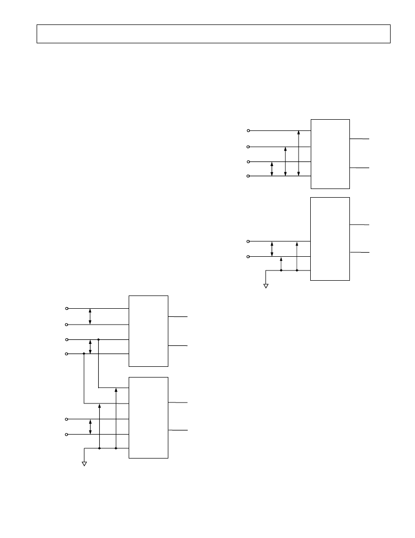
Figure 16 shows the analog input channel configurations avail-
able to the user when the CHCON bit in the mode register is set
to a zero. In this case the main ADC can be configured as one
or two fully differential input channels (AIN1/AIN2 and AIN3/
AIN4) and the aux can be configured as two single-ended inputs
with respect to AGND (AIN3/AGND and AIN4/AGND) and
one fully differential input AIN5/AIN6). The aux can also be
configured as three single-ended inputs with respect to AGND
(AIN3/AGND, AIN4/AGND and AIN5/AGND) by tying AIN6
externally to AGND. The temp sensor is available as an internal
connection.
SINGLE-
ENDED
INPUT
SINGLE-
ENDED
INPUT
FULLY DIFFERENTIAL
FULLY DIFFERENTIAL
FULLY DIFFERENTIAL
AIN(+)
AIN(
–
)
AIN(+)
AIN(
–
)
AIN1
AIN2
AIN3
AIN4
AIN1
AIN2
AIN3
AIN4
AIN5
AIN6
AIN3
AIN4
AGND
MUX1
(MAIN ADC)
(AUX ADC)
AIN5
AIN6
MAIN CHANNEL
AUX CHANNEL
MUX2
Figure 16. Input Channel Configurations with CHCON = 0
Figure 17 shows the analog input channel configurations avail-
able to the user when the CHCON bit in the mode register is
set to a one. In this case the main ADC is configured as three
pseudo-differential input channels (AIN1/AIN4, AIN2/AIN4,
and AIN3/AIN4) and the aux can be configured as two single-
ended inputs with respect to AGND (AIN5/AGND and AIN6/
AGND) and one fully differential input AIN5/AIN6). The temp
sensor is available as an internal connection.
SINGLE-
ENDED
INPUT
FULLY DIFFERENTIAL
AIN(+)
AIN(
–
)
AIN(+)
AIN(
–
)
AIN1
AIN2
AIN3
AIN4
AIN1
AIN2
AIN3
AIN4
AIN5
AIN6
AIN3
AIN4
AGND
(AUX ADC)
MUX1
(MAIN ADC)
AIN5
AIN6
SINGLE-
ENDED
INPUT
AIN3/AIN4
AIN2/AIN4
AIN1/AIN4
MUX2
MAIN CHANNEL
AUX CHANNEL
PSEUDO-
DIFFERENTIAL
INPUT
PSEUDO-
DIFFERENTIAL
INPUT
Figure 17. Input Channel Configurations with CHCON = 1
In buffered mode (
BUF
= 0), the output of the main ADC multi-
plexer feeds into a high-impedance input stage of the buffer
amplifier. As a result, the main ADC inputs can handle significant
source impedances and are tailored for direct connection to
external resistive-type sensors like strain gages or Resistance
Temperature Detectors (RTDs).
The auxiliary ADC and the main ADC when operated with
BUF
= 1, however, are unbuffered resulting in higher analog
input current. It should be noted that these unbuffered input
paths provide a dynamic load to the driving source. Therefore,
resistor/capacitor combinations on the input pins can cause dc
gain errors depending on the output impedance of the source
that is driving the ADC inputs. Table XVIII and XIX show the
allowable external resistance/capacitance values for unbuffered
mode such that no gain error at the 16- and 20-bit level respectively
is introduced.
The absolute input voltage range on the main ADC when oper-
ated in buffered mode is restricted to a range between AGND +
100 mV and AV
DD
–
100 mV. Care must be taken in setting up
the common-mode voltage and input voltage range so that these
limits are not exceeded; otherwise there will be a degradation in
linearity and noise performance.
相關(guān)PDF資料 |
PDF描述 |
|---|---|
| AD7719BR | Low Voltage, Low Power, Factory-Calibrated 16-/24-Bit Dual ADC |
| AD7720 | CMOS Sigma-Delta Modulator |
| AD7720BRU | CMOS Sigma-Delta Modulator |
| AD7721 | CMOS 16-Bit, 468.75 kHz, Sigma-Delta ADC |
| AD7721AN | CMOS 16-Bit, 468.75 kHz, Sigma-Delta ADC |
相關(guān)代理商/技術(shù)參數(shù) |
參數(shù)描述 |
|---|---|
| AD7719BR | 制造商:Analog Devices 功能描述:ADC Dual Delta-Sigma 105sps 24-bit Serial 28-Pin SOIC W 制造商:Rochester Electronics LLC 功能描述:DUAL 16-BIT & 24-BIT SD ADC - Bulk 制造商:Analog Devices 功能描述:Analog-Digital Converter IC Number of Bi |
| AD7719BR-REEL | 功能描述:IC ADC 16BIT 24BIT DUAL 28-SOIC RoHS:否 類別:集成電路 (IC) >> 數(shù)據(jù)采集 - 模數(shù)轉(zhuǎn)換器 系列:- 標(biāo)準(zhǔn)包裝:1,000 系列:- 位數(shù):12 采樣率(每秒):300k 數(shù)據(jù)接口:并聯(lián) 轉(zhuǎn)換器數(shù)目:1 功率耗散(最大):75mW 電壓電源:單電源 工作溫度:0°C ~ 70°C 安裝類型:表面貼裝 封裝/外殼:24-SOIC(0.295",7.50mm 寬) 供應(yīng)商設(shè)備封裝:24-SOIC 包裝:帶卷 (TR) 輸入數(shù)目和類型:1 個單端,單極;1 個單端,雙極 |
| AD7719BR-REEL7 | 功能描述:IC ADC 16BIT 24BIT DUAL 28-SOIC RoHS:否 類別:集成電路 (IC) >> 數(shù)據(jù)采集 - 模數(shù)轉(zhuǎn)換器 系列:- 標(biāo)準(zhǔn)包裝:1,000 系列:- 位數(shù):12 采樣率(每秒):300k 數(shù)據(jù)接口:并聯(lián) 轉(zhuǎn)換器數(shù)目:1 功率耗散(最大):75mW 電壓電源:單電源 工作溫度:0°C ~ 70°C 安裝類型:表面貼裝 封裝/外殼:24-SOIC(0.295",7.50mm 寬) 供應(yīng)商設(shè)備封裝:24-SOIC 包裝:帶卷 (TR) 輸入數(shù)目和類型:1 個單端,單極;1 個單端,雙極 |
| AD7719BRU | 制造商:Analog Devices 功能描述:ADC Dual Delta-Sigma 105sps 24-bit Serial 28-Pin TSSOP |
| AD7719BRU-REEL | 制造商:Analog Devices 功能描述:ADC Dual Delta-Sigma 105sps 24-bit Serial 28-Pin TSSOP T/R 制造商:Analog Devices 功能描述:ADC DUAL DELTA-SIGMA 0.105KSPS 24BIT SERL 28TSSOP - Tape and Reel |
發(fā)布緊急采購,3分鐘左右您將得到回復(fù)。