- 您現(xiàn)在的位置:買賣IC網(wǎng) > PDF目錄373915 > AD7720BRU (ANALOG DEVICES INC) CMOS Sigma-Delta Modulator PDF資料下載
參數(shù)資料
| 型號(hào): | AD7720BRU |
| 廠商: | ANALOG DEVICES INC |
| 元件分類: | ADC |
| 英文描述: | CMOS Sigma-Delta Modulator |
| 中文描述: | 1-CH 16-BIT DELTA-SIGMA ADC, SERIAL ACCESS, PDSO28 |
| 封裝: | TSSOP-28 |
| 文件頁(yè)數(shù): | 10/16頁(yè) |
| 文件大小: | 232K |
| 代理商: | AD7720BRU |
第1頁(yè)第2頁(yè)第3頁(yè)第4頁(yè)第5頁(yè)第6頁(yè)第7頁(yè)第8頁(yè)第9頁(yè)當(dāng)前第10頁(yè)第11頁(yè)第12頁(yè)第13頁(yè)第14頁(yè)第15頁(yè)第16頁(yè)
AD7720
–10–
REV. 0
CIRCUIT DE SCRIPT ION
Sigma-Delta ADC
T he AD7720 ADC employs a sigma-delta conversion technique
that converts the analog input into a digital pulse train. T he
analog input is continuously sampled by a switched capacitor
modulator at twice the rate of the clock input frequency (2
×
f
MCLK
). T he digital data that represents the analog input is in
the one’s density of the bit stream at the output of the sigma-
delta modulator. T he modulator outputs the bit stream at a data
rate equal to f
MCLK
.
Due to the high oversampling rate, which spreads the quantiza-
tion noise from 0 to f
MCLK
/2, the noise energy contained in the
band of interest is reduced (Figure 21a). T o reduce the quanti-
zation noise further, a high order modulator is employed to
shape the noise spectrum, so that most of the noise energy is
shifted out of the band of interest (Figure 21b).
BAND OF INTEREST
QUANTIZATION NOISE
f
MCLK
/2
BAND OF INTEREST
NOISE SHAPING
a.
b.
f
MCLK
/2
Figure 21. Sigma-Delta ADC
USING T HE AD7720
ADC Differential Inputs
T he AD7720 uses differential inputs to provide common-mode
noise rejection (i.e., the converted result will correspond to the
differential voltage between the two inputs). T he absolute volt-
age on both inputs must lie between AGND and AVDD.
In the unipolar mode, the full-scale input range (VIN(+) –
VIN(–)) is 0 V to V
REF
. In the bipolar mode configuration, the
full-scale analog input range is
±
V
REF2
/2. T he bipolar mode
allows complementary input signals. Alternatively, VIN(–) can
be connected to a dc bias voltage to allow a single-ended input
on VIN(+) equal to V
BIAS
±
V
REF2
/2.
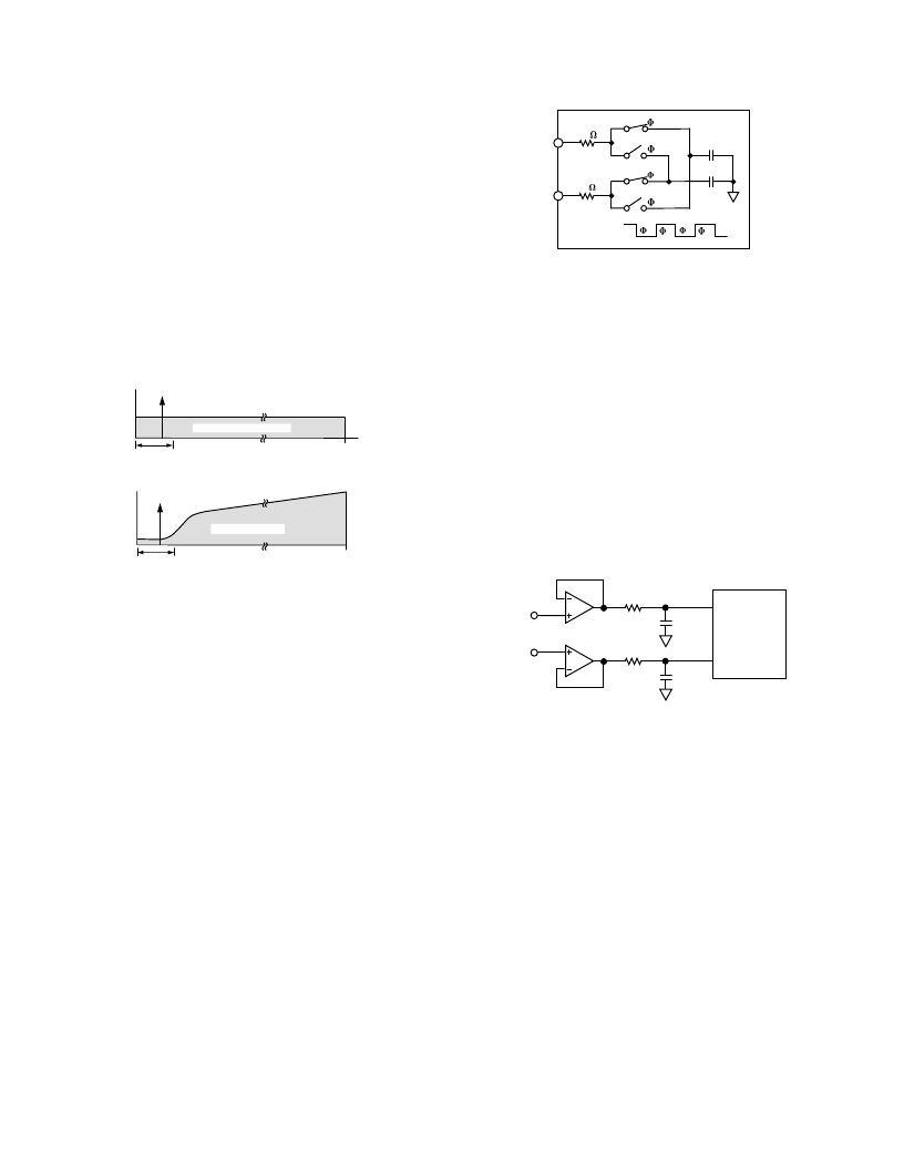
Differential Inputs
T he analog input to the modulator is a switched capacitor de-
sign. T he analog input is converted into charge by highly linear
sampling capacitors. A simplified equivalent circuit diagram of
the analog input is shown in Figure 22. A signal source driving
the analog input must be able to provide the charge onto the
sampling capacitors every half MCLK cycle and settle to the
required accuracy within the next half cycle.
A
B
A
B
2pF
2pF
AC
GROUND
500
A
B
A
B
MCLK
VIN(+)
VIN(–)
500
Figure 22. Analog Input Equivalent Circuit
Since the AD7720 samples the differential voltage across its
analog inputs, low noise performance is attained with an input
circuit that provides low differential mode noise at each input.
T he amplifiers used to drive the analog inputs play a critical
role in attaining the high performance available from the AD7720.
When a capacitive load is switched onto the output of an op
amp, the amplitude will momentarily drop. T he op amp will try
to correct the situation and, in the process, hits its slew rate
limit. T his nonlinear response, which can cause excessive ring-
ing, can lead to distortion. T o remedy the situation, a low pass
RC filter can be connected between the amplifier and the input
to the AD7720 as shown in Figure 23. T he external capacitor
at each input aids in supplying the current spikes created during
the sampling process. T he resistor in this diagram, as well as
creating the pole for the antialiasing, isolates the op amp from
the transient nature of the load.
ANALOG
INPUT
R
C
VIN(+)
VIN(–)
R
C
Figure 23. Simple RC Antialiasing Circuit
T he differential input impedance of the AD7720 switched
capacitor input varies as a function of the MCLK frequency,
given by the equation:
Z
IN
= 10
9
/(8
f
MCLK
)
k
Even though the voltage on the input sampling capacitors may
not have enough time to settle to the accuracy indicated by the
resolution of the AD7720, as long as the sampling capacitor
charging follows the exponential curve of RC circuits, only the
gain accuracy suffers if the input capacitor is switched away too
early.
An alternative circuit configuration for driving the differential
inputs to the AD7720 is shown in Figure 24.
相關(guān)PDF資料 |
PDF描述 |
|---|---|
| AD7721 | CMOS 16-Bit, 468.75 kHz, Sigma-Delta ADC |
| AD7721AN | CMOS 16-Bit, 468.75 kHz, Sigma-Delta ADC |
| AD7721AR | CMOS 16-Bit, 468.75 kHz, Sigma-Delta ADC |
| AD7721SQ | CMOS 16-Bit, 468.75 kHz, Sigma-Delta ADC |
| AD7722 | 16-Bit, 195 kSPS CMOS, Sigma-Delta ADC |
相關(guān)代理商/技術(shù)參數(shù) |
參數(shù)描述 |
|---|---|
| AD7720BRU-REEL | 制造商:Analog Devices 功能描述:ADC Single Delta-Sigma 25Msps 16-bit Serial 28-Pin TSSOP T/R |
| AD7720BRU-REEL7 | 制造商:Analog Devices 功能描述:ADC Single Delta-Sigma 25Msps 16-bit Serial 28-Pin TSSOP T/R 制造商:Rochester Electronics LLC 功能描述:- Tape and Reel |
| AD7720BRUZ | 功能描述:IC MODULATOR SIGMA-DELTA 28TSSOP RoHS:是 類別:集成電路 (IC) >> 數(shù)據(jù)采集 - 模數(shù)轉(zhuǎn)換器 系列:- 標(biāo)準(zhǔn)包裝:1,000 系列:- 位數(shù):12 采樣率(每秒):300k 數(shù)據(jù)接口:并聯(lián) 轉(zhuǎn)換器數(shù)目:1 功率耗散(最大):75mW 電壓電源:單電源 工作溫度:0°C ~ 70°C 安裝類型:表面貼裝 封裝/外殼:24-SOIC(0.295",7.50mm 寬) 供應(yīng)商設(shè)備封裝:24-SOIC 包裝:帶卷 (TR) 輸入數(shù)目和類型:1 個(gè)單端,單極;1 個(gè)單端,雙極 |
| AD7720BRUZ-REEL | 功能描述:IC MODULATOR SIGMA-DELTA 28TSSOP RoHS:是 類別:集成電路 (IC) >> 數(shù)據(jù)采集 - 模數(shù)轉(zhuǎn)換器 系列:- 標(biāo)準(zhǔn)包裝:1,000 系列:- 位數(shù):12 采樣率(每秒):300k 數(shù)據(jù)接口:并聯(lián) 轉(zhuǎn)換器數(shù)目:1 功率耗散(最大):75mW 電壓電源:單電源 工作溫度:0°C ~ 70°C 安裝類型:表面貼裝 封裝/外殼:24-SOIC(0.295",7.50mm 寬) 供應(yīng)商設(shè)備封裝:24-SOIC 包裝:帶卷 (TR) 輸入數(shù)目和類型:1 個(gè)單端,單極;1 個(gè)單端,雙極 |
| AD7720BRUZ-REEL7 | 功能描述:IC MODULATOR SIGMA-DELTA 28TSSOP RoHS:是 類別:集成電路 (IC) >> 數(shù)據(jù)采集 - 模數(shù)轉(zhuǎn)換器 系列:- 標(biāo)準(zhǔn)包裝:1,000 系列:- 位數(shù):12 采樣率(每秒):300k 數(shù)據(jù)接口:并聯(lián) 轉(zhuǎn)換器數(shù)目:1 功率耗散(最大):75mW 電壓電源:單電源 工作溫度:0°C ~ 70°C 安裝類型:表面貼裝 封裝/外殼:24-SOIC(0.295",7.50mm 寬) 供應(yīng)商設(shè)備封裝:24-SOIC 包裝:帶卷 (TR) 輸入數(shù)目和類型:1 個(gè)單端,單極;1 個(gè)單端,雙極 |
發(fā)布緊急采購(gòu),3分鐘左右您將得到回復(fù)。