- 您現在的位置:買賣IC網 > PDF目錄373915 > AD7729 (Analog Devices, Inc.) Dual Sigma-Delta ADC with Auxiliary DAC PDF資料下載
參數資料
| 型號: | AD7729 |
| 廠商: | Analog Devices, Inc. |
| 英文描述: | Dual Sigma-Delta ADC with Auxiliary DAC |
| 中文描述: | 雙Σ-Δ型ADC輔助DAC |
| 文件頁數: | 11/16頁 |
| 文件大小: | 142K |
| 代理商: | AD7729 |
AD7729
–11–
REV. 0
10
0
–10
–20
–30
–40
–50
–60
–70
–80
–90
–100
–110
–120
0
150
200
250
100
50
300
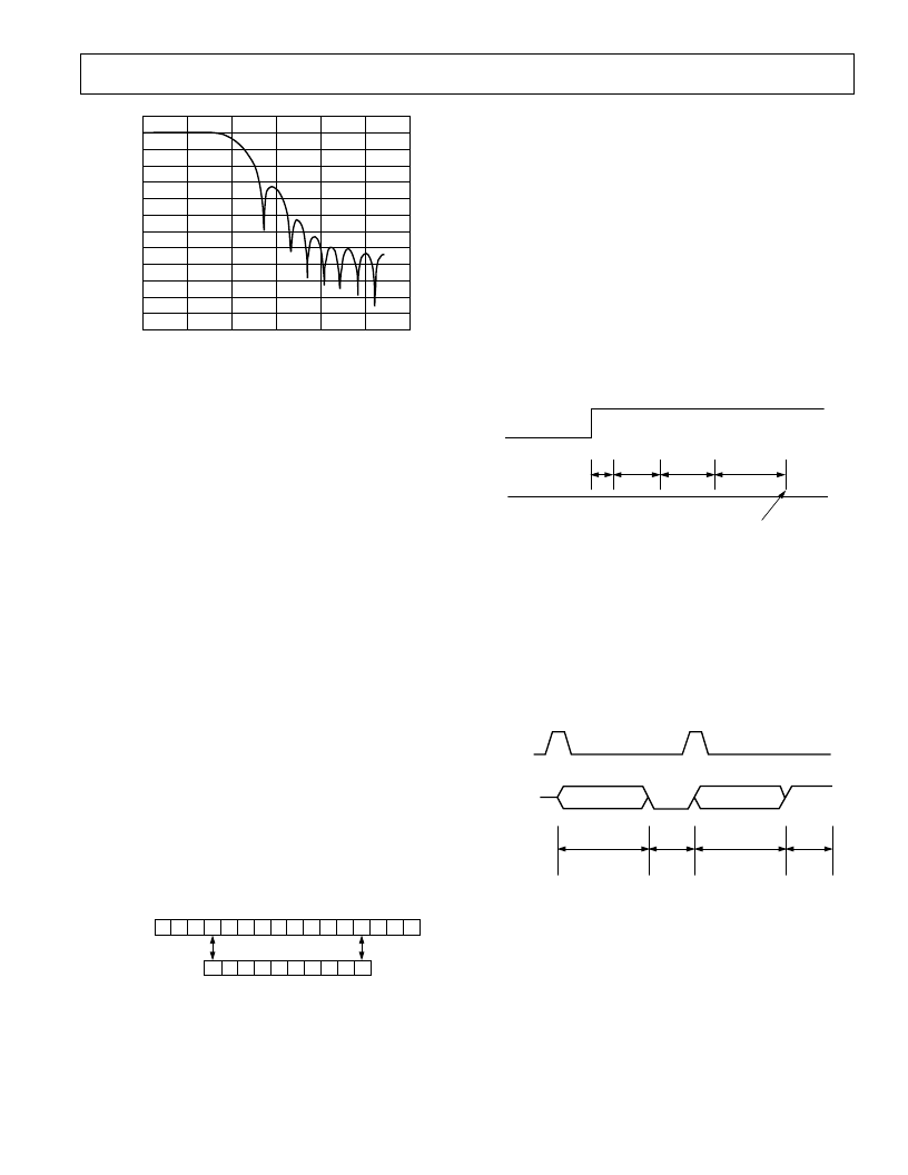
FREQUENCY – kHz
G
Figure 14. Digital Filter Frequency Response
Filter Characteristics
The digital filter is a 288-tap FIR filter, clocked at half the mas-
ter clock frequency. The 3 dB point is at 96 kHz.
Due to the low-pass nature of the receive filters, a settling time
is associated with step input functions. Output data will not be
meaningful until all the digital filter taps have been loaded
with data samples taken after the step change. Hence the AD7729
digital filters have a settling time of 44.7
μ
s (288
×
2t
1
).
Receive Offset Calibration
Included in the digital filter is a means by which receive offsets
may be calibrated out. Each channel of the digital low-pass filter
section has an offset register. The offset register can be made to
contain a value representing the dc offset of the preceding ana-
log circuitry. In normal operation, the value stored in the offset
register is subtracted from the filter output data before the data
appears on the serial output pin. By so doing, dc offsets in the I
and Q channels are calibrated out. Autocalibration or user-
calibration can be selected. Internal autocalibration will remove
internal offsets only while user calibration allows the user to
write to the offset register in order to also remove external offsets.
The offset registers have enough resolution to hold the value of
any dc offset between
±
162.5 mV (1/8th of the input range).
Offsets larger than
±
162.5 mV will cause a spurious result due to
calibration overrange. However, the performance of the sigma-
delta modulators will degrade if full-scale signals with more than
100 mV of offset are experienced. The 10-bit offset register
represents a twos complement value. The LSB of the offset
registers corresponds to Bit 3 of the Rx words while the MSB of
the offset registers corresponds to Bit 12 of the Rx words (see
Figure 15).
RxDATA
OFFSET REGISTER
15 14 13 12 11 10
9
8
7
6
5
4
3 2
1
0
9
8
7
6
5
4
3 2
1
0
Figure 15. Position of the 10-Bit Offset Word
Receive Offset Adjust: Autocalibration
If receive autocalibration is selected, the AD7729 will initiate an
autocalibration routine each time the receive path is brought out
of the low power sleep mode. After RxON is asserted, by taking
the RxON bit or the RxON pin high, 36 symbol periods are
allowed for the analog and digital circuitry to settle. An internal
timer then times out a time equal to RxDELAY1.
When RxDELAY1 has expired, the AD7729 offset calibration
routine begins, assuming the RxAUTOCAL bit in control regis-
ter BCRA is equal to 1. If RxAUTOCAL equals zero, no cali-
bration occurs and T2 in Figure 16 equals zero. In internal
autocalibration mode, the AD7729 internally disconnects the
differential inputs from the input pins and shorts the inputs to
measure the resulting ADC offset. In external autocalibration
mode, the inputs remain connected to the pins, allowing system
offsets along with the AD7729 internal offsets to be evaluated.
This is then averaged 16 times to reduce noise and the averaged
result is then placed in the offset register. The input to the ADC
is then switched back for normal operation and the analog cir-
cuitry and digital filter are permitted to settle. This time period
is included in T
CALIBRATE
, which equals 40
×
48 MCLK cycles.
RxON
T0
T1
T2
FIRST VALID OUTPUT WORD HERE
T0 = T
SETTLE
= 36
3
48 MCLKs
T1 = RxDELAY1 = 0...255
3
48 MCLKs
T2 = T
CALIBRATE
= 40
3
48 MCLKs
T3 = RxDELAY2 = 0...255
3
48 MCLKs
T3
Figure 16. Data Rx Procedure
After calibration is complete, a second timer is started which
times out a time equal to RxDELAY2. The range of both
RxDELAY1 and RxDELAY2 is 0 to 255 units where each unit
equals one bit time. Therefore, the maximum delay time is
255
×
1/270 kHz = 941.55
μ
s.
As soon as RxDELAY2 has expired, valid output words appear
at the output. The Rx data will be 15 bits wide.
ASDOFS
BSDOFS
ASDO
BSDO
VALID I DATA
I FLAG
VALID Q DATA
Q FLAG
T1
T2
I WORD
Q WORD
T2
T1
T1 = 16 MCLKs
T2 = 8 MCLKs
Figure 17. ASDO/BSDO in Rx Mode
Receive Offset Adjust: User Calibration
When user calibration is selected, the receive offset register can
be written to, allowing offsets in the IF/RF demodulation cir-
cuitry to be calibrated out also. However, the user is now re-
sponsible for calibrating out receive offsets belonging to the
AD7729. When the receive path enters the low power mode, the
registers remain valid. After powering up, the first IQ sample
pair is output once time has elapsed for both the analog circuitry
to settle and also for the output of the digital filter to settle.
相關PDF資料 |
PDF描述 |
|---|---|
| AD7729AR | Dual Sigma-Delta ADC with Auxiliary DAC |
| AD7729ARU | Dual Sigma-Delta ADC with Auxiliary DAC |
| AD7730LBR | Bridge Transducer ADC |
| AD7730LBRU | Bridge Transducer ADC |
| AD7730 | Bridge Transducer ADC |
相關代理商/技術參數 |
參數描述 |
|---|---|
| AD7729AR | 制造商:Analog Devices 功能描述:ADC Dual Delta-Sigma 13Msps 15-bit Serial 28-Pin SOIC W 制造商:Rochester Electronics LLC 功能描述:3DUAL SIGMA DELTA ADC I.C. - Bulk 制造商:Analog Devices 功能描述:ADC DUAL SIGMA DELTA 7729 SOIC28 |
| AD7729AR-REEL7 | 制造商:Analog Devices 功能描述:ADC Dual Delta-Sigma 13Msps 15-bit Serial 28-Pin SOIC W T/R |
| AD7729ARU | 功能描述:IC ADC 15BIT DUAL W/DAC 28-TSSOP RoHS:否 類別:集成電路 (IC) >> 數據采集 - ADCs/DAC - 專用型 系列:- 產品培訓模塊:Lead (SnPb) Finish for COTS Obsolescence Mitigation Program 標準包裝:50 系列:- 類型:數據采集系統(DAS) 分辨率(位):16 b 采樣率(每秒):21.94k 數據接口:MICROWIRE?,QSPI?,串行,SPI? 電壓電源:模擬和數字 電源電壓:1.8 V ~ 3.6 V 工作溫度:-40°C ~ 85°C 安裝類型:表面貼裝 封裝/外殼:40-WFQFN 裸露焊盤 供應商設備封裝:40-TQFN-EP(6x6) 包裝:托盤 |
| AD7729ARU-REEL | 功能描述:IC ADC 15BIT DUAL W/DAC 28-TSSOP RoHS:否 類別:集成電路 (IC) >> 數據采集 - ADCs/DAC - 專用型 系列:- 產品培訓模塊:Lead (SnPb) Finish for COTS Obsolescence Mitigation Program 標準包裝:50 系列:- 類型:數據采集系統(DAS) 分辨率(位):16 b 采樣率(每秒):21.94k 數據接口:MICROWIRE?,QSPI?,串行,SPI? 電壓電源:模擬和數字 電源電壓:1.8 V ~ 3.6 V 工作溫度:-40°C ~ 85°C 安裝類型:表面貼裝 封裝/外殼:40-WFQFN 裸露焊盤 供應商設備封裝:40-TQFN-EP(6x6) 包裝:托盤 |
| AD7729ARU-REEL7 | 功能描述:IC ADC 15BIT DUAL W/DAC 28-TSSOP RoHS:否 類別:集成電路 (IC) >> 數據采集 - ADCs/DAC - 專用型 系列:- 產品培訓模塊:Lead (SnPb) Finish for COTS Obsolescence Mitigation Program 標準包裝:50 系列:- 類型:數據采集系統(DAS) 分辨率(位):16 b 采樣率(每秒):21.94k 數據接口:MICROWIRE?,QSPI?,串行,SPI? 電壓電源:模擬和數字 電源電壓:1.8 V ~ 3.6 V 工作溫度:-40°C ~ 85°C 安裝類型:表面貼裝 封裝/外殼:40-WFQFN 裸露焊盤 供應商設備封裝:40-TQFN-EP(6x6) 包裝:托盤 |
發布緊急采購,3分鐘左右您將得到回復。