- 您現在的位置:買賣IC網 > PDF目錄373915 > AD773AJD (ANALOG DEVICES INC) 10-Bit, 20 MSPS Monolithic A/D Converter PDF資料下載
參數資料
| 型號: | AD773AJD |
| 廠商: | ANALOG DEVICES INC |
| 元件分類: | ADC |
| 英文描述: | 10-Bit, 20 MSPS Monolithic A/D Converter |
| 中文描述: | 1-CH 10-BIT PROPRIETARY METHOD ADC, PARALLEL ACCESS, CDIP28 |
| 封裝: | CERAMIC, DIP-28 |
| 文件頁數: | 10/16頁 |
| 文件大小: | 223K |
| 代理商: | AD773AJD |
AD773A
REV. 0
–10–
OUT PUT DAT A FORMAT
T he AD773A provides both MSB and
MSB
outputs, delivering
positive true offset binary and twos complement output data.
T able II shows the AD773A’s output data format.
T able II. Output Data Format
Analog Input
Digital Output
T wos
Complement
Offset
Binary
V
INA
–V
INB
OT R
≥
499.5 mV
499 mV
0 mV
–500 mV
≤
–500.5 mV
11 1111 1111
11 1111 1111
10 0000 0000
00 0000 0000
00 0000 0000
01 1111 1111
01 1111 1111
00 0000 0000
10 0000 0000
10 0000 0000
1
0
0
0
1
OUT OF RANGE
An out-of-range condition exists when the analog input voltage
is beyond the input range (
±
500 mV) of the converter. [Note
the AD773A has a 4 clock cycle latency.] OT R (Pin 20) is set
low when the analog input voltage is within the analog input
range. OT R is set HIGH and will remain HIGH when the
analog input voltage exceeds the input range by 1/2 LSB from
the center of the
±
full-scale output codes. OT R will remain
HIGH until the analog input is within the input range. Note
that if the input is driven beyond +1.5 V, the digital outputs
may not stay at +FS, but may actually fold back to midscale. By
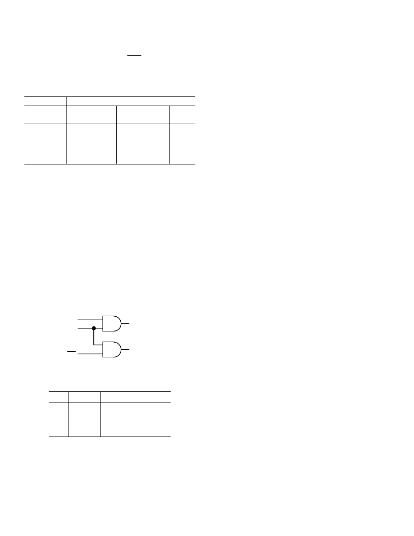
logical ANDing OT R with the MSB and its complement,
overrange high or underrange low conditions can be detected.
T able III is a truth table for the over/under range circuit in
Figure 20. Systems requiring programmable gain conditioning
prior to the AD773A can immediately detect an out of range
condition, thus eliminating gain selection iterations.
MSB
OTR
OVER = "1"
UNDER = "1"
MSB
Figure 20. Overrange or Underrange Logic
T able III. Out-of-Range T ruth T able
OT R
MSB
ANALOG INPUT IS
0
0
1
1
0
1
0
1
In Range
In Range
Underrange
Overrange
GROUNDING AND LAY OUT RULE S
As is the case for any high performance device, proper
grounding and layout techniques are essential in achieving
optimal performance. (Note—Figures 22–26 are not to scale.)
T he analog and digital grounds on the AD773A have been
separated to optimize the management of return currents in a
system. It is recommended that a 4-layer printed circuit board
(PCB) which employs ground planes and power planes be used
with the AD773A. T he use of ground and power planes offers
distinct advantages:
1. T he minimization of the loop area encompassed by a signal
and its return path.
2. T he minimization of the impedance associated with ground
and power paths.
3. T he inherent distributed capacitor formed by the power
plane, PCB insulation, and ground plane.
T hese characteristics result in both a reduction of electro-
magnetic interference (EMI) and an overall improvement
in performance.
It is important to design a layout which prevents noise from
coupling onto the input signal. T he wide input bandwidth of the
AD773A permits noise outside the desired Nyquist bandwidth
to be sampled along with the desired signal. T his can result in a
higher overall level of spurious noise in the digitized output.
Digital signals should not be run in parallel with the circuitry. It
is also suggested that the traces associated with V
INA
and V
INB
be
the same length.
Separate analog and digital grounds should be joined together
directly under the AD773A (see Figure 24). A solid ground
plane under the AD773A is also acceptable if care is taken in
the management of the power and ground return currents. A
general “rule-of-thumb” for mixed signal layouts dictates that
the return currents from digital circuitry should not pass
through critical analog circuitry.
POWE R SUPPLY DE COUPLING
T he analog and digital supplies of the AD773A have been
separated to prevent the typically large transients associated with
digital circuitry from coupling into the analog supplies (AV
DD
,
AV
SS
). Each analog power supply pin should be decoupled with
a 0.1
μ
F capacitor located as close to the pin as possible.
Additionally, 0.22
μ
F capacitors for the DRV
DD
and DV
DD
supplies are required to adequately suppress high frequency
noise. For optimal performance, surface-mount capacitors are
recommended. T he inductance associated with the leads of
through-hole ceramic capacitors typically render them
ineffective at higher frequencies. A
complete
system will also
incorporate tantalum capacitors in the 10–100
μ
F range to
decouple low frequency noise and ferrite beads to limit high
frequency noise.
T he digital supplies have also been separated into DRV
DD
and
DV
DD
. T he DRV
DD
pins provide power for the digital output
drivers of the AD773A and are likely to contain high energy
transients. Pin 22 should be decoupled directly to Pin 21
(DRGND) and Pin 7 should be decoupled directly to Pin 8
(DRGND) to minimize the length of the return path for these
transients. A single +5 V supply is all that is required for
DRV
DD
and DV
DD
, but decoupling DV
DD
with an RC filter
network is suggested (see Figure 21).
相關PDF資料 |
PDF描述 |
|---|---|
| AD773AKD | 10-Bit, 20 MSPS Monolithic A/D Converter |
| AD7740KRM | 3 V/5 V Low Power, Synchronous Voltage-to-Frequency Converter |
| AD7740YRT | 3 V/5 V Low Power, Synchronous Voltage-to-Frequency Converter |
| AD7740 | 3 V/5 V Low Power, Synchronous Voltage-to-Frequency Converter |
| AD7740YRM | 3 V/5 V Low Power, Synchronous Voltage-to-Frequency Converter |
相關代理商/技術參數 |
參數描述 |
|---|---|
| AD773AKD | 制造商:AD 制造商全稱:Analog Devices 功能描述:10-Bit, 20 MSPS Monolithic A/D Converter |
| AD773ASD/883B | 制造商:未知廠家 制造商全稱:未知廠家 功能描述:Analog-to-Digital Converter, 10-Bit |
| AD773-EB | 制造商:Rochester Electronics LLC 功能描述:- Bulk |
| AD773JD | 制造商:Analog Devices 功能描述: |
| AD773KD | 制造商:未知廠家 制造商全稱:未知廠家 功能描述:Analog-to-Digital Converter, 10-Bit |
發布緊急采購,3分鐘左右您將得到回復。