- 您現在的位置:買賣IC網 > PDF目錄373915 > AD773AJD (ANALOG DEVICES INC) 10-Bit, 20 MSPS Monolithic A/D Converter PDF資料下載
參數資料
| 型號: | AD773AJD |
| 廠商: | ANALOG DEVICES INC |
| 元件分類: | ADC |
| 英文描述: | 10-Bit, 20 MSPS Monolithic A/D Converter |
| 中文描述: | 1-CH 10-BIT PROPRIETARY METHOD ADC, PARALLEL ACCESS, CDIP28 |
| 封裝: | CERAMIC, DIP-28 |
| 文件頁數: | 9/16頁 |
| 文件大小: | 223K |
| 代理商: | AD773AJD |
AD773A
REV. 0
–9–
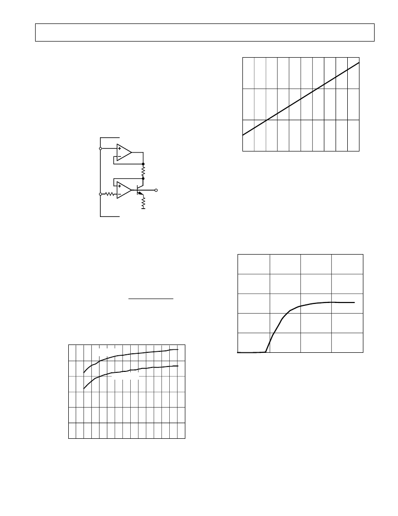
E QUIVALE NT RE FE RE NCE INPUT CIRCUIT
T he AD773A is designed to have a reference to analog input
voltage ratio of 2.5:1. When the AD773A is configured for
single-ended operation a 2.5 volt reference input establishes a
full-scale analog input voltage of 1 V p-p (
±
500 mV with respect
to V
INB
). Although the AD773A is specified and tested with
V
REF
equal to 2.5 V and V
IN
equal to
±
500 mV the reference
input voltage and analog input voltages can be changed. T o
optimize the AD773A’s performance the 2.5:1 ratio should be
maintained. T he simplified model of the AD773A’s reference
input circuit is shown in Figure 16.
REFIN
REFGND
R3
R1
R2
V
–5V
A
BIAS
AD773A
Figure 16. Typical Reference Input Circuit
T he 2.5 V external reference is applied across resistor R1
producing a current which in turn generates a voltage V
BIAS
.
Multiple reference currents are generated from V
BIAS
and are
used throughout the converter. R3 is used to cancel errors
induced by the input bias current of the REFGND buffer.
Figure 17 shows the SNR performance as the reference voltage
is varied from its nominal value of 2.5 V. T he input full-scale
voltage is defined by the following equation,
Input Full-Scale Voltage =
T he power dissipation is modulated by variations in the
reference voltage. Figure 18 shows the variation in power
dissipation versus reference voltage.
ReferenceVoltage
2.5
60
30
45
35
40
55
50
1.0
3.8
3.0
2.6
2.2
1.8
REFERENCE INPUT VOLTAGE – V
1.4
3.4
S
AIN = –0.3dB
AIN = –6dB
Figure 17. S/N+D vs. Reference Input Voltage,
f
CLK
= 20 MSPS, f
IN
= 1 MHz
1.2
0.9
3.0
1.1
1
2
REFIN – V
P
2.6
2.4
2.2
2.8
2.7
2.5
2.3
2.1
2.9
Figure 18. Power Dissipation vs. Reference Input
Voltage, f
CLOCK
= 20 MSPS
T RANSIE NT RE SPONSE
T he fast settling input T HA accurately converts full-scale input
voltage swings in under one clock cycle. T he T HA’s high
impedance, fast slewing performance is critical in multiplexed or
dc stepped (charge coupled devices, infrared detectors) systems.
Figure 19 show the AD773A’s settling performance with an
input signal stepped from –500 mV to 0 V. As can be seen, the
output code settles to its final value in under one clock cycle.
0
0
TIME – ns
C
40
600
200
10
400
1000
800
30
20
CODE
Figure 19. Typical AD773A Settling Time
相關PDF資料 |
PDF描述 |
|---|---|
| AD773AKD | 10-Bit, 20 MSPS Monolithic A/D Converter |
| AD7740KRM | 3 V/5 V Low Power, Synchronous Voltage-to-Frequency Converter |
| AD7740YRT | 3 V/5 V Low Power, Synchronous Voltage-to-Frequency Converter |
| AD7740 | 3 V/5 V Low Power, Synchronous Voltage-to-Frequency Converter |
| AD7740YRM | 3 V/5 V Low Power, Synchronous Voltage-to-Frequency Converter |
相關代理商/技術參數 |
參數描述 |
|---|---|
| AD773AKD | 制造商:AD 制造商全稱:Analog Devices 功能描述:10-Bit, 20 MSPS Monolithic A/D Converter |
| AD773ASD/883B | 制造商:未知廠家 制造商全稱:未知廠家 功能描述:Analog-to-Digital Converter, 10-Bit |
| AD773-EB | 制造商:Rochester Electronics LLC 功能描述:- Bulk |
| AD773JD | 制造商:Analog Devices 功能描述: |
| AD773KD | 制造商:未知廠家 制造商全稱:未知廠家 功能描述:Analog-to-Digital Converter, 10-Bit |
發布緊急采購,3分鐘左右您將得到回復。