- 您現在的位置:買賣IC網 > PDF目錄373916 > AD7769JP (ANALOG DEVICES INC) LC2MOS Analog I/O Port PDF資料下載
參數資料
| 型號: | AD7769JP |
| 廠商: | ANALOG DEVICES INC |
| 元件分類: | ADC |
| 英文描述: | LC2MOS Analog I/O Port |
| 中文描述: | 2-CH 8-BIT SUCCESSIVE APPROXIMATION ADC, PARALLEL ACCESS, PQCC28 |
| 封裝: | PLASTIC, LCC-28 |
| 文件頁數: | 8/16頁 |
| 文件大小: | 265K |
| 代理商: | AD7769JP |
AD7769
–8–
REV. A
CIRCUIT DE SCRIPT ION
Analog Inputs and Outputs
T he AD7769 provides the analog-to-digital and digital-to-analog
conversion functions required between the microcontroller and
the servo power amplifier in digital servo systems. It is intended
primarily for closed loop head positioning in Winchester disk
drives, but may also be used for microstepping in drives with
stepper motor head positioning or other servo applications. T he
AD7769 contains a high speed, 8-bit, sampling ADC with two
input channels and two 8-bit DACs with output buffer amplifi-
ers. A unique feature of the AD7769 is the input and output sig-
nal conditioning circuitry that allows the analog input and
output voltages to be referred to a point other than analog
ground. T he input range and offset of the ADC, the output
swing and offset of the DACs may be adjusted independently by
the application of ground-referenced, positive control voltages,
V
BIAS
(ADC), V
SWING
(ADC), V
BIAS
(DAC) and V
SWING
(DAC).
T hus, for example, the peak-to-peak output swing of the DACs
could be set to 3 V above and 3 V below a bias voltage of 5 V.
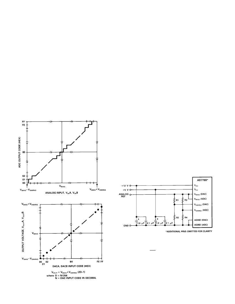
Figures 5 and 6 show the transfer functions of the ADC
and DACs and their relationship to V
BIAS
and V
SWING.
T he
Figure 5. ADC Transfer Function
Figure 6. DAC Transfer Function
midpoint code of the ADC, 80 Hex (10000000 Binary), occurs
at an input voltage equal to V
BIAS
. T he input FSR of the ADC is
equal to 2 V
SWING
, so that the Plus Full-Scale code transition
(FE to FF Hex) occurs at a voltage equal to V
BIAS
+ V
SWING
–1.5 LSBs and the Minus Full-Scale code transition (01 to 00
Hex) occurs at a voltage V
BIAS
– V
SWING
+0.5 LSBs. T he
transfer function of the DACs bears a similar relationship to
V
BIAS
and V
SWING
. T he DAC output voltage for code 80 Hex
(10000000 binary) is equal to V
BIAS
, while FF Hex (11111111
binary) gives an output voltage of V
BIAS
+ V
SWING
–1 LSB
(Plus Full-Scale) and 00 Hex gives an output voltage of V
BIAS
–
V
SWING
(Minus Full-Scale).
T he ability to refer input and output signals to some voltage
other than ground is of particular importance in disk drive ap-
plications. T ypically, only +5 V digital and +12 V analog supply
voltages are available, and the analog signals are often referred
to a voltage around half the analog supply.
Driving the Analog Inputs and Reference Inputs
T he analog inputs, V
IN
A and V
IN
B, must be driven from low
output impedance sources, such as from op amps. In addition,
V
BIAS
(ADC) must be driven from a similar type low impedance
source (e.g., voltage reference).
Op amps are not required to drive the V
SWING
(ADC), V
BIAS
(DAC) and V
SWING
(DAC) inputs as these are high impedance
inputs (200 nA typical input current) that feed into on-chip
buffer amplifiers. T he reference voltages for these inputs can be
derived using suitable resistor divider networks.
T he analog reference available in the disk drive system can be
used to set the bias voltage of the AD7769, and could also be at-
tenuated to provide the reference for the input and output swing
as shown in Figure 7. T he same bias voltage would generally
(though not necessarily) be used for the ADC and the DACs,
though the input and output ranges might be different.
Figure 7. Typical Analog Connections to the AD7769
ADC Conversion Cycle
Figure 8 shows the operating waveforms for a conversion cycle.
On the rising edge of
WR
, the conversion cycle starts with the
acquisition and tracking of the selected ADC channel, V
IN
A or
V
IN
B. T he analog input voltage is held 50 ns (typically) after the
fourth falling edge of the input CLK following a conversion
start. If t
D
in Figure 8 is greater than 150 ns, then the falling
edge of the input CLK will be seen as the first falling clock edge.
If t
D
is less than 150 ns, the first falling clock edge to be recog-
nized will not occur until one cycle later.
相關PDF資料 |
PDF描述 |
|---|---|
| AD7773 | LC MOS COMPLETE EMBEDDED SERVO FRONT ENDS FOR HDD |
| AD7775 | LC MOS COMPLETE EMBEDDED SERVO FRONT ENDS FOR HDD |
| AD7776 | LC2MOS, High Speed 1-, 4- & 8-Channel 10-Bit ADCs |
| AD7776AR | LC2MOS, High Speed 1-, 4- & 8-Channel 10-Bit ADCs |
| AD7777 | LC2MOS, High Speed 1-, 4- & 8-Channel 10-Bit ADCs |
相關代理商/技術參數 |
參數描述 |
|---|---|
| AD7769JP-REEL | 制造商:Rochester Electronics LLC 功能描述:- Tape and Reel |
| AD7769KN | 制造商:未知廠家 制造商全稱:未知廠家 功能描述:CODEC, Single |
| AD7769KP | 制造商:未知廠家 制造商全稱:未知廠家 功能描述:CODEC, Single |
| AD776AQ | 制造商:未知廠家 制造商全稱:未知廠家 功能描述:Analog-to-Digital Converter, 16-Bit |
| AD7770ACPZ | 功能描述:24 Bit Analog to Digital Converter 8 Input 8 Sigma-Delta 64-LFCSP (9x9) 制造商:analog devices inc. 系列:- 包裝:托盤 零件狀態:有效 位數:24 采樣率(每秒):32k 輸入數:8 輸入類型:差分,單端 數據接口:SPI 配置:MUX-PGA-ADC 無線電 - S/H:ADC:- A/D 轉換器數:8 架構:三角積分 參考類型:外部, 內部 電壓 - 電源,模擬:2.2 V ~ 3.6 V 電壓 - 電源,數字:- 特性:PGA,同步采樣 工作溫度:-40°C ~ 125°C 封裝/外殼:64-WFQFN 裸露焊盤,CSP 供應商器件封裝:64-LFCSP(9x9) 標準包裝:1 |
發布緊急采購,3分鐘左右您將得到回復。