- 您現在的位置:買賣IC網 > PDF目錄373916 > AD7776AR (ANALOG DEVICES INC) LC2MOS, High Speed 1-, 4- & 8-Channel 10-Bit ADCs PDF資料下載
參數資料
| 型號: | AD7776AR |
| 廠商: | ANALOG DEVICES INC |
| 元件分類: | ADC |
| 英文描述: | LC2MOS, High Speed 1-, 4- & 8-Channel 10-Bit ADCs |
| 中文描述: | 1-CH 10-BIT PROPRIETARY METHOD ADC, PARALLEL ACCESS, PDSO24 |
| 封裝: | MS-013AD, SOIC-24 |
| 文件頁數: | 5/12頁 |
| 文件大小: | 220K |
| 代理商: | AD7776AR |
AD7776/AD7777/AD7778
–5–
REV. 0
PIN FUNCT ION DE SCRIPT ION
Mnemonic
Description
V
CC
AGND
DGND
DB0–DB9
+5 V Power Supply.
Analog Ground.
Digital Ground. Ground reference for digital circuitry.
Input/Output Data Bus. T his is a bidirectional data port from which ADC output data may be read and to which
control register data may be written.
Busy/Interrupt Output. Active low logic output indicating A/D converter status. T his logic output has two modes
of operation depending on whether location CR9 of the control register has been set low or high:
If CR9 is set low, then the
BUSY
/
INT
output will behave as a
BUSY
signal. T he
BUSY
signal will go low and stay
low for the duration of a single conversion, or if simultaneous sampling has been selected,
BUSY
will stay low for
the duration of both conversions.
If CR9 is set high, then the
BUSY
/
INT
output behaves as an INT ERRUPT signal. T he
INT
signal will go low
and remain low after either a single conversion is completed or after a double conversion is completed if simulta-
neous sampling has been selected. With CR9 high, the falling edge of
WR
or
RD
resets the
INT
line high.
Chip Select Input. T he device is selected when this input is low.
Write Input (Active Low). It is used in conjunction with
CS
to write data to the control register. Data is latched to the
registers on the rising edge of
WR
. Following the rising edge of
WR
, the analog input is acquired and a conversion is
started.
Read Input (Active Low). It is used in conjunction with
CS
to enable the data outputs from the ADC registers.
Analog Inputs 1–8. T he analog input range is V
BIAS
±
V
SWING
where V
BIAS
and V
SWING
are defined by the reference
voltage applied to REFIN. Input resistance between any of the analog input pins and AGND is 10 k
or greater.
Voltage Reference Input. T he AD7776/AD7777/AD7778 are specified over a voltage reference range of 1.9 V to 2.1 V
with a nominal value of 2.0 V. T his REFIN voltage provides the V
BIAS
and V
SWING
levels for the input channel(s).
V
BIAS
is equal to REFIN and V
SWING
is nominally equal to REFIN/2. Input resistance between this REFIN pin and
AGND is 10 k
or greater.
Voltage Reference Output. T he internal voltage reference, which is nominally 2.0 V and can be used to provide the
bias voltage (V
BIAS
) for the input channel(s), is provided at this pin.
Reference Decoupling Capacitor. A 10 nF capacitor must be connected from this pin to AGND to ensure correct
operation of the high speed ADC.
Signal Return Path for the input channel(s). Normally RT N is connected to AGND at the package.
BUSY
/
INT
CS
WR
RD
A
IN
1–8
REFIN
REFOUT
C
REFIN
RT N
CIRCUIT DE SCRIPT ION
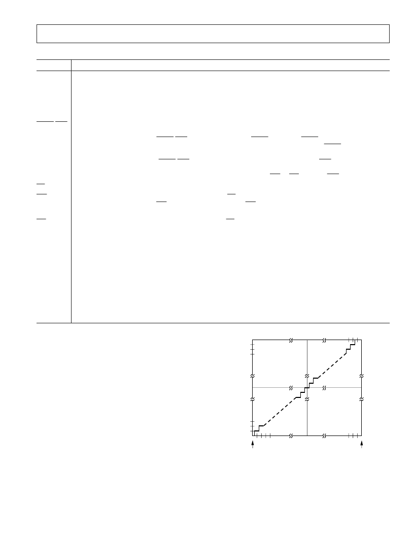
ADC T ransfer Function
For all versions, an input signal of the form V
BIAS
±
V
SWING
is
expected. T his V
BIAS
signal level operates as a pseudo ground to
which all input signals must be referred. T he V
BIAS
level is de-
termined by the voltage applied to the REFIN pin. T his can be
driven by an external voltage source or, alternatively, the on-
board 2 V reference, available at REFOUT , can be used. T he
magnitude of the input signal swing is equal to V
BIAS
/2 (or
REFIN/2) and is set internally. With a REFIN of 2 V, the analog
input signal level varies from 1 V up to 3 V i.e., 2
±
1 V. Fig-
ure 5 shows the transfer function of the ADC and its relation-
ship to V
BIAS
and V
SWING
. T he half-scale twos complement code
of the ADC, 000 Hex (00 0000 0000 Binary), occurs at an input
voltage equal to V
BIAS
. T he input full-scale range of the ADC is
equal to 2 V
SWING
, so that the Plus Full-Scale transition (1FE to
1FF) occurs at a voltage equal to V
BIAS
+ V
SWING
– 1.5 LSBs
and the minus full-scale code transition (200 to 201) occurs at
a voltage V
BIAS
– V
SWING
+ 0.5 LSBs.
ADC
OUTPUT
CODE
(HEX)
1FF
1FE
202
201
200
000
V
BIAS
–V
SWING
V
BIAS
V
BIAS
+V
SWING
ANALOG INPUT, V
IN
Figure 5. ADC Transfer Function
相關PDF資料 |
PDF描述 |
|---|---|
| AD7777 | LC2MOS, High Speed 1-, 4- & 8-Channel 10-Bit ADCs |
| AD7777AN | LC2MOS, High Speed 1-, 4- & 8-Channel 10-Bit ADCs |
| AD7777AR | LC2MOS, High Speed 1-, 4- & 8-Channel 10-Bit ADCs |
| AD7778 | LC2MOS, High Speed 1-, 4- & 8-Channel 10-Bit ADCs |
| AD7778AS | LC2MOS, High Speed 1-, 4- & 8-Channel 10-Bit ADCs |
相關代理商/技術參數 |
參數描述 |
|---|---|
| AD7776AR-REEL | 功能描述:IC ADC 10BIT 1CH HS 24-SOIC T/R RoHS:否 類別:集成電路 (IC) >> 數據采集 - 模數轉換器 系列:- 標準包裝:1,000 系列:- 位數:12 采樣率(每秒):300k 數據接口:并聯 轉換器數目:1 功率耗散(最大):75mW 電壓電源:單電源 工作溫度:0°C ~ 70°C 安裝類型:表面貼裝 封裝/外殼:24-SOIC(0.295",7.50mm 寬) 供應商設備封裝:24-SOIC 包裝:帶卷 (TR) 輸入數目和類型:1 個單端,單極;1 個單端,雙極 |
| AD7776ARZ | 功能描述:IC ADC 10BIT 1CHAN HS 24SOIC RoHS:是 類別:集成電路 (IC) >> 數據采集 - 模數轉換器 系列:- 產品培訓模塊:Lead (SnPb) Finish for COTS Obsolescence Mitigation Program 標準包裝:2,500 系列:- 位數:12 采樣率(每秒):3M 數據接口:- 轉換器數目:- 功率耗散(最大):- 電壓電源:- 工作溫度:- 安裝類型:表面貼裝 封裝/外殼:SOT-23-6 供應商設備封裝:SOT-23-6 包裝:帶卷 (TR) 輸入數目和類型:- |
| AD7776ARZ-REEL | 功能描述:IC ADC 10BIT 1CHAN HS 24SOIC RoHS:是 類別:集成電路 (IC) >> 數據采集 - 模數轉換器 系列:- 標準包裝:1,000 系列:- 位數:12 采樣率(每秒):300k 數據接口:并聯 轉換器數目:1 功率耗散(最大):75mW 電壓電源:單電源 工作溫度:0°C ~ 70°C 安裝類型:表面貼裝 封裝/外殼:24-SOIC(0.295",7.50mm 寬) 供應商設備封裝:24-SOIC 包裝:帶卷 (TR) 輸入數目和類型:1 個單端,單極;1 個單端,雙極 |
| AD7777 | 制造商:AD 制造商全稱:Analog Devices 功能描述:LC2MOS, High Speed 1-, 4- & 8-Channel 10-Bit ADCs |
| AD7777AN | 制造商:Analog Devices 功能描述:ADC Single SAR 378ksps 10-bit Parallel 28-Pin PDIP 制造商:Analog Devices 功能描述:4 CH 10-BIT ADC IC - Rail/Tube 制造商:Rochester Electronics LLC 功能描述:4 CH 10-BIT ADC IC - Bulk |
發布緊急采購,3分鐘左右您將得到回復。