- 您現在的位置:買賣IC網 > PDF目錄373916 > AD7776AR (ANALOG DEVICES INC) LC2MOS, High Speed 1-, 4- & 8-Channel 10-Bit ADCs PDF資料下載
參數資料
| 型號: | AD7776AR |
| 廠商: | ANALOG DEVICES INC |
| 元件分類: | ADC |
| 英文描述: | LC2MOS, High Speed 1-, 4- & 8-Channel 10-Bit ADCs |
| 中文描述: | 1-CH 10-BIT PROPRIETARY METHOD ADC, PARALLEL ACCESS, PDSO24 |
| 封裝: | MS-013AD, SOIC-24 |
| 文件頁數: | 9/12頁 |
| 文件大小: | 220K |
| 代理商: | AD7776AR |
AD7776/AD7777/AD7778
–9–
REV. 0
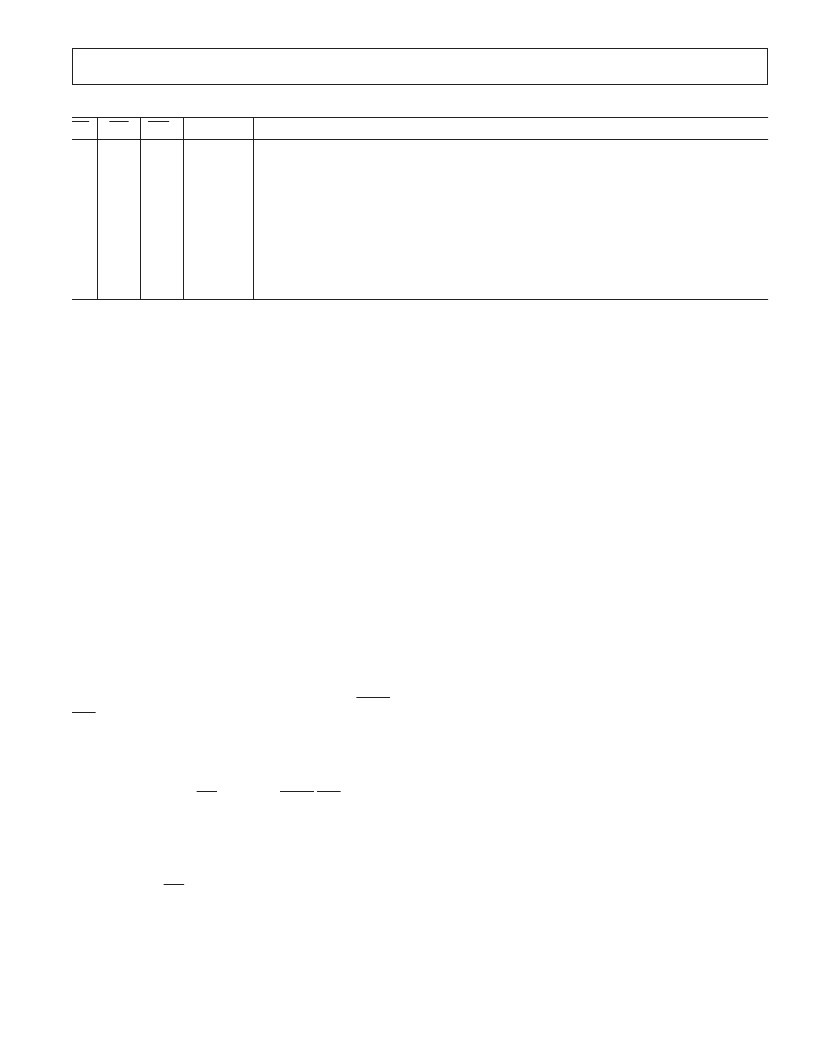
T able I. AD7776/AD7777/AD7778 T ruth T able for Microprocessor Interfacing
CS
RD
WR
DB0–DB9
Function/Comments
1
0
0
X *
1
X *
High Z
CR Data
ADC Data
Data Port High Impedance
Load control register (CR) data to control register and start a conversion.
ADC data placed on data bus. Depending upon location CR6 of the control register, one or two
Read instructions will be required.
If CR6 is low, i.e., single channel conversion selected, a read instruction returns the contents of
ADCREG1. Succeeding read instructions continue to return the contents of ADCREG1.
If CR6 is high, i.e., simultaneous sampling (double conversion) selected, the first read instruction
returns the contents of ADCREG1 while the second read instruction returns the contents of
ADCREG2. A third read instruction returns ADCREG1 again, the fourth ADCREG2, etc.
j
1
k
*X = Don’t Care
DE SIGN INFORMAT ION
Layout Hints
Ensure that the layout for the printed circuit board has the digi-
tal and analog grounds separated as much as possible. T ake care
not to run any digital track alongside an analog signal track.
Guard (screen) the analog input(s) with RT N.
Establish a single point analog ground separate from the logic
system ground and as close as possible to the AD7776/AD7777/
AD7778. Both the RT N and AGND pins on the AD7776/
AD7777/AD7778 and all other signal grounds should be con-
nected to this single point analog ground. In turn, this star
ground should be connected to the digital ground at one point
only—preferably at the low impedance power supply itself.
Low impedance analog and digital power supply common re-
turns are important for correct operation of the devices, so make
the foil width for these tracks as wide as possible.
In order to ensure a low impedance +5 V power supply at the
actual V
CC
pin, it will be necessary to employ bypass capacitors
from the pin itself to DGND. A 4.7
μ
F tantalum capacitor in
parallel with a 0.1
μ
F ceramic capacitor is sufficient.
ADC Corruption
Executing a read instruction to the AD7776/AD7777/AD7778
while a conversion is in progress will immediately halt the con-
version and return invalid data over the data bus. T he
BUSY
/
INT
output pin should be monitored closely and all read in-
structions to the AD7776/AD7777/AD7778 prevented while
this output shows that a conversion is in progress.
Executing a write instruction to the AD7776/AD7777/AD7778
while a conversion is in progress immediately halts the conver-
sion, the falling edge of
WR
driving the
BUSY
/
INT
output high.
T he analog input(s) is sampled as normal and a new conversion
sequence (dependent upon CR6) is started.
ADC Conversion T ime
Although each conversion takes only 14 CLK IN cycles, it can
take between 4.5 to 5.5 CLK IN cycles to acquire the analog
input(s) after the
WR
input goes high and before any conver-
sions start.
T E RMINOLOGY
Relative Accuracy
For the AD7776, AD7777 and AD7778, relative accuracy or
endpoint nonlinearity is the maximum deviation, in LSBs, of the
ADC’s actual code transition points from a straight line drawn
between the endpoints of the ADC transfer function.
Differential Nonlinearity
Differential nonlinearity is the difference between the measured
change and the ideal 1 LSB change between any two adjacent
codes. A specified maximum differential nonlinearity of
±
1 LSB
ensures no missed codes.
Bias Offset E rror
For an ideal 10-bit ADC, the output code for an input voltage
equal to V
BIAS
should be midscale. T he bias offset error is the
difference between the actual midpoint voltage for midscale
code and V
BIAS
, expressed in LSBs.
Bias Offset E rror Match
T his is a measure of how closely the bias offset errors of all
channels track each other. T he bias offset error match of any
channel must be no further away than 10 LSBs from the bias
offset error of any other channel, regardless of whether the
channels are independently sampled or simultaneously sampled.
Plus and Minus Full-Scale E rror
T he input channels of the ADC can be considered to have
bipolar (positive and negative) input ranges, but which are re-
ferred to V
BIAS
(or REFIN) instead of AGND. Positive full-scale
error for the ADC is the difference between the actual input
voltage required to produce the plus full-scale code transition
and the ideal input voltage (V
BIAS
+ V
SWING
–1.5 LSB), ex-
pressed in LSBs. Minus full-scale error is similarly specified for
the minus full-scale code transition, relative to the ideal input
voltage for this transition (V
BIAS
– V
SWING
+ 0.5 LSB). Note that
the full-scale errors for the ADC input channels are measured
after their respective bias offset errors have been adjusted out.
Plus and Minus Full-Scale E rror Match
T his is a measure of how closely the full-scale errors of all chan-
nels track each other. T he full-scale error match of any channel
must be no further away than 10 LSBs from the respective full-
scale error of any other channel, regardless of whether the chan-
nels are independently sampled or simultaneously sampled.
相關PDF資料 |
PDF描述 |
|---|---|
| AD7777 | LC2MOS, High Speed 1-, 4- & 8-Channel 10-Bit ADCs |
| AD7777AN | LC2MOS, High Speed 1-, 4- & 8-Channel 10-Bit ADCs |
| AD7777AR | LC2MOS, High Speed 1-, 4- & 8-Channel 10-Bit ADCs |
| AD7778 | LC2MOS, High Speed 1-, 4- & 8-Channel 10-Bit ADCs |
| AD7778AS | LC2MOS, High Speed 1-, 4- & 8-Channel 10-Bit ADCs |
相關代理商/技術參數 |
參數描述 |
|---|---|
| AD7776AR-REEL | 功能描述:IC ADC 10BIT 1CH HS 24-SOIC T/R RoHS:否 類別:集成電路 (IC) >> 數據采集 - 模數轉換器 系列:- 標準包裝:1,000 系列:- 位數:12 采樣率(每秒):300k 數據接口:并聯 轉換器數目:1 功率耗散(最大):75mW 電壓電源:單電源 工作溫度:0°C ~ 70°C 安裝類型:表面貼裝 封裝/外殼:24-SOIC(0.295",7.50mm 寬) 供應商設備封裝:24-SOIC 包裝:帶卷 (TR) 輸入數目和類型:1 個單端,單極;1 個單端,雙極 |
| AD7776ARZ | 功能描述:IC ADC 10BIT 1CHAN HS 24SOIC RoHS:是 類別:集成電路 (IC) >> 數據采集 - 模數轉換器 系列:- 產品培訓模塊:Lead (SnPb) Finish for COTS Obsolescence Mitigation Program 標準包裝:2,500 系列:- 位數:12 采樣率(每秒):3M 數據接口:- 轉換器數目:- 功率耗散(最大):- 電壓電源:- 工作溫度:- 安裝類型:表面貼裝 封裝/外殼:SOT-23-6 供應商設備封裝:SOT-23-6 包裝:帶卷 (TR) 輸入數目和類型:- |
| AD7776ARZ-REEL | 功能描述:IC ADC 10BIT 1CHAN HS 24SOIC RoHS:是 類別:集成電路 (IC) >> 數據采集 - 模數轉換器 系列:- 標準包裝:1,000 系列:- 位數:12 采樣率(每秒):300k 數據接口:并聯 轉換器數目:1 功率耗散(最大):75mW 電壓電源:單電源 工作溫度:0°C ~ 70°C 安裝類型:表面貼裝 封裝/外殼:24-SOIC(0.295",7.50mm 寬) 供應商設備封裝:24-SOIC 包裝:帶卷 (TR) 輸入數目和類型:1 個單端,單極;1 個單端,雙極 |
| AD7777 | 制造商:AD 制造商全稱:Analog Devices 功能描述:LC2MOS, High Speed 1-, 4- & 8-Channel 10-Bit ADCs |
| AD7777AN | 制造商:Analog Devices 功能描述:ADC Single SAR 378ksps 10-bit Parallel 28-Pin PDIP 制造商:Analog Devices 功能描述:4 CH 10-BIT ADC IC - Rail/Tube 制造商:Rochester Electronics LLC 功能描述:4 CH 10-BIT ADC IC - Bulk |
發布緊急采購,3分鐘左右您將得到回復。