- 您現在的位置:買賣IC網 > PDF目錄373916 > AD7787BRM (ANALOG DEVICES INC) Low Power, 2-Channel 24-Bit Sigma-Delta ADC PDF資料下載
參數資料
| 型號: | AD7787BRM |
| 廠商: | ANALOG DEVICES INC |
| 元件分類: | ADC |
| 英文描述: | Low Power, 2-Channel 24-Bit Sigma-Delta ADC |
| 中文描述: | 2-CH 24-BIT DELTA-SIGMA ADC, SERIAL ACCESS, PDSO10 |
| 封裝: | MO-187BA, MSOP-10 |
| 文件頁數: | 15/20頁 |
| 文件大小: | 326K |
| 代理商: | AD7787BRM |
AD7787
DIGITAL INTERFACE
As previously outlined, the AD7787’s programmable functions
are controlled using a set of on-chip registers. Data is written to
these registers via the part’s serial interface and read access to
the on-chip registers is also provided by this interface. All
communications with the part must start with a write to the
communications register. After power-on or reset, the device
expects a write to its communications register. The data written
to this register determines whether the next operation is a read
operation or a write operation and also determines to which
register this read or write operation occurs. Therefore, write
access to any of the other registers on the part begins with a
write operation to the communications register followed by a
write to the selected register. A read operation from any other
register (except when continuous read mode is selected) starts
with a write to the communications register followed by a read
operation from the selected register.
Rev. 0 | Page 15 of 20
The AD7787’s serial interface consists of four signals: CS, DIN,
SCLK, and DOUT/RDY. The DIN line is used to transfer data
into the on-chip registers while DOUT/RDY is used for
accessing data from the on-chip registers. SCLK is the serial
clock input for the device and all data transfers (either on DIN
or DOUT/RDY) occur with respect to the SCLK signal.
The DOUT/ RDY pin operates as a data-ready signal as well as
a DOUT pin. Each time a conversion is available in the output
register, DOUT/RDY goes low. DOUT/RDY resets high when a
read operation from the data register is completed. It also goes
high prior to the updating of the data register to indicate when
not to read from the device to ensure that a data read is not
attempted while the register is being updated. CS is used to
select a device. It can be used to decode the AD7787 in systems
where several components are connected to the serial bus.
Figure 3 and Figure 4 show timing diagrams for interfacing to
the AD7787 with CS being used to decode the part. Figure 3
shows the timing for a read operation from the AD7787’s output
shift register, while Figure 4 shows the timing for a write
operation to the input shift register. In all modes, except
continuous read mode, it is possible to read the same word from
the data register several times even though the DOUT/RDY line
returns high after the first read operation. However, care must be
taken to ensure that the read operations have been completed
before the next output update occurs. In continuous read mode, the
data register can only be read once.
The serial interface can operate in 3-wire mode by tying CS low.
In this case, the SCLK, DIN, and DOUT/RDY lines are used to
communicate with the AD7787. The end of the conversion can
be monitored using the RDY bit in the status register. This
scheme is suitable for interfacing to microcontrollers. If CS is
required as a decoding signal, it can be generated from a port
pin. For microcontroller interfaces, it is recommended that
SCLK idle high between data transfers.
The AD7787 can be operated with CS being used as a frame
synchronization signal. This scheme is useful for DSP interfaces.
In this case, the first bit (MSB) is effectively clocked out by CS,
because CS would normally occur after the falling edge of SCLK
in DSPs. The SCLK can continue to run between data transfers,
provided the timing numbers are obeyed.
The serial interface can be reset by writing a series of 1s to the
DIN input. If a Logic 1 is written to the AD7787 line for at least
32 serial clock cycles, the serial interface is reset. In 3-wire
systems, this ensures that the interface can be reset to a known
state if the interface gets lost due to a software error or some
glitch in the system. Reset returns the interface to the state in
which it is expecting a write to the communications register.
This operation resets the contents of all registers to their power-
on values.
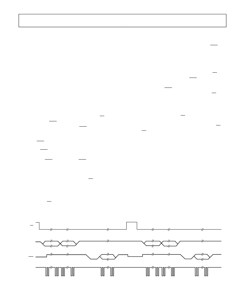
The AD7787 can be configured to continuously convert or to
perform a single conversion (see Figure 13 through Figure 15).
0
DIN
0x10
0x82
0x10
0x82
DATA
DATA
SCLK
DOUT/RDY
CS
Figure 13. Single Conversion
相關PDF資料 |
PDF描述 |
|---|---|
| AD7787BRM-REEL | Low Power, 2-Channel 24-Bit Sigma-Delta ADC |
| AD7787 | Low Power, 2-Channel 24-Bit Sigma-Delta ADC |
| AD7789 | Low Power, 16-/24-Bit Sigma-Delta ADC |
| AD7788 | Low Power, 16-/24-Bit Sigma-Delta ADC |
| AD7788ARM | Low Power, 16-/24-Bit Sigma-Delta ADC |
相關代理商/技術參數 |
參數描述 |
|---|---|
| AD7787BRM-REEL | 功能描述:IC ADC 24BIT LP 2CH SIG 10-MSOP RoHS:否 類別:集成電路 (IC) >> 數據采集 - 模數轉換器 系列:- 標準包裝:1,000 系列:- 位數:16 采樣率(每秒):45k 數據接口:串行 轉換器數目:2 功率耗散(最大):315mW 電壓電源:模擬和數字 工作溫度:0°C ~ 70°C 安裝類型:表面貼裝 封裝/外殼:28-SOIC(0.295",7.50mm 寬) 供應商設備封裝:28-SOIC W 包裝:帶卷 (TR) 輸入數目和類型:2 個單端,單極 |
| AD7787BRMZ | 功能描述:IC ADC 24BIT 2CH LP SIG 10MSOP RoHS:是 類別:集成電路 (IC) >> 數據采集 - 模數轉換器 系列:- 標準包裝:1,000 系列:- 位數:16 采樣率(每秒):45k 數據接口:串行 轉換器數目:2 功率耗散(最大):315mW 電壓電源:模擬和數字 工作溫度:0°C ~ 70°C 安裝類型:表面貼裝 封裝/外殼:28-SOIC(0.295",7.50mm 寬) 供應商設備封裝:28-SOIC W 包裝:帶卷 (TR) 輸入數目和類型:2 個單端,單極 |
| AD7787BRMZ | 制造商:Analog Devices 功能描述:IC 24BIT ADC SMD 7787 MSOP10 |
| AD7787BRMZ-RL | 功能描述:IC ADC 24BIT 2CH LP SIG 10MSOP RoHS:是 類別:集成電路 (IC) >> 數據采集 - 模數轉換器 系列:- 標準包裝:1,000 系列:- 位數:16 采樣率(每秒):45k 數據接口:串行 轉換器數目:2 功率耗散(最大):315mW 電壓電源:模擬和數字 工作溫度:0°C ~ 70°C 安裝類型:表面貼裝 封裝/外殼:28-SOIC(0.295",7.50mm 寬) 供應商設備封裝:28-SOIC W 包裝:帶卷 (TR) 輸入數目和類型:2 個單端,單極 |
| AD7788 | 制造商:AD 制造商全稱:Analog Devices 功能描述:Low Power, 16-/24-Bit Sigma-Delta ADC |
發布緊急采購,3分鐘左右您將得到回復。