- 您現在的位置:買賣IC網 > PDF目錄373918 > AD7834 (Analog Devices, Inc.) 14-Bit Quad DAC(14位四D/A轉換器) PDF資料下載
參數資料
| 型號: | AD7834 |
| 廠商: | Analog Devices, Inc. |
| 英文描述: | 14-Bit Quad DAC(14位四D/A轉換器) |
| 中文描述: | 14位四路DAC(14位四的D / A轉換器) |
| 文件頁數: | 10/16頁 |
| 文件大小: | 416K |
| 代理商: | AD7834 |
REV. A
–10–
AD7834/AD7835
Table IV. Code Table for Unipolar Operation
Binary Number in DAC Latch
MSB
Analog Output
(V
OUT
)
LSB
11
10
01
00
00
1111
0000
1111
0000
0000
1111
0000
1111
0000
0000
1111
0000
1111
0001
0000
V
REF
(16383/16384) V
V
REF
(8192/16384) V
V
REF
(8191/16384) V
V
REF
(1/16384) V
0 V
NOTE
V
= V
(+); V
(–) = 0 V for unipolar operation.
For V
REF
(+) = +5 V, 1 LSB = +5 V/2
14
= +5 V/16384 = 305
μ
V.
Bipolar Configuration
Figure 14 shows the AD7834/AD7835 set up for
±
5 V opera-
tion. The AD588 provides precision
±
5 V tracking outputs
which are fed to the V
REF
(+) and V
REF
(–) inputs of the AD7834/
AD7835. The code table for bipolar operation of the AD7834/
AD7835 is shown in Table V.
+15V
+5V
V
(–5 TO +5V)
V
CC
6
3
4
C1
1μF
AGND
DGND
V
DD
V
OUT
V
REF
(+)
V
REF
(–)
V
SS
–15V
*
ADDITIONAL PINS OMITTED FOR CLARITY
R2
100k
AD7834/
AD7835
*
SIGNAL
GND
2
14
15
16
12
8
13
11
10
5
9
7
R3
100k
R1
1
AD588
Figure 14. Bipolar
±
5 V Operation
Table V. Code Table for Bipolar Operation
Binary Number in DAC Latch Analog Output
MSB
LSB
(V
OUT
)
11
10
10
01
00
00
1111
0000
0000
1111
0000
0000
1111
0000
0000
1111
0000
0000
1111
0001
0000
1111
0001
0000
V
REF
(–) + V
REF
(16383/16384) V
V
REF
(–) + V
REF
(8193/16384) V
V
REF
(–) + V
REF
(8192/16384) V
V
REF
(–) + V
REF
(8191/16384) V
V
REF
(–) + V
REF
(1/16384) V
V
REF
(–) V
NOTE
V
REF
= (V
REF
(+) – V
REF
(–)).
For V
REF
(+) = +5 V, and V
REF
(–) = –5 V, 1 LSB = 10 V/2
14
= 10 V/16384 =
610
μ
V.
In Figure 14, full-scale and bipolar zero adjustments are pro-
vided by varying the gain and balance on the AD588. R2 varies
the gain on the AD588 while R3 adjusts the offset of both the
+5 V and –5 V outputs together with respect to ground.
For bipolar-zero adjustment, the DAC is loaded with
1000 . . . 0000 and R3 is adjusted until V
OUT
= 0 V. Full scale
is adjusted by loading the DAC with all 1s and adjusting R2 un-
til V
OUT
= 5(8191/8192) V = 4.99939 V.
When bipolar-zero and full-scale adjustment are not needed, R2
and R3 can be omitted. Pin 12 on the AD588 should be con-
nected to Pin 11 and Pin 5 should be left floating.
When 14-bit transfers are being used, the DAC output voltages,
V
OUT
1–V
OUT
4, can be updated to reflect new data in the DAC
input registers in one of two ways. The first method normally
keeps
LDAC
high and only pulses
LDAC
low momentarily to
update all DAC latches simultaneously with the contents of
their respective input registers. The second method ties
LDAC
low and channel updating occurs on a per channel basis after
new data is loaded to an input register.
In order to avoid the DAC output going to an intermediate
value during a 2-byte transfer,
LDAC
should not be tied low
permanently, but should be held high until the 2 bytes are writ-
ten to the input register. When the selected input register has
been loaded with the 2 bytes,
LDAC
should then be pulsed low
to update the DAC latch and, hence, perform the digital-to-
analog conversion.
In many applications, it may be acceptable to allow the DAC
output to go to an intermediate value during a 2-byte transfer.
In such applications,
LDAC
can be tied low, thus using one less
control line.
The actual DAC input register that is being written to is deter-
mined by the logic levels present on the devices address lines, as
shown in Table III.
Table III. AD7835—Address Line Truth Table
A2
A1
A0
DAC Selected
0
0
0
0
1
0
0
1
1
X
0
1
0
1
X
DAC 1
DAC 2
DAC 3
DAC 4
All DACs Selected
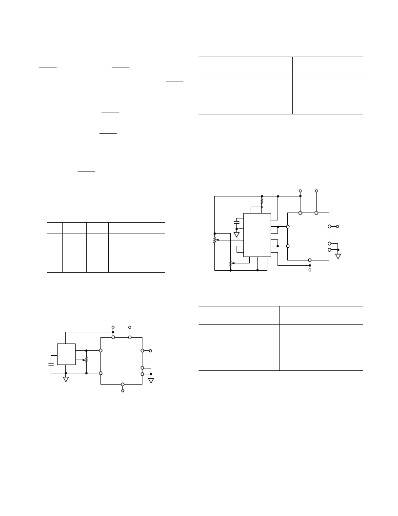
Unipolar Configuration
Figure 13 shows the AD7834/AD7835 in the unipolar binary
circuit configuration. The V
REF
(+) input of the DAC is driven
by the AD586, a +5 V reference. V
REF
(–) is tied to ground.
Table IV gives the code table for unipolar operation of the
AD7834/AD7835.
+15V
+5V
V
(0 TO +5V)
V
CC
2
6
8
5
4
SIGNAL
GND
C1
1nF
AGND
DGND
V
DD
V
OUT
V
REF
(+)
V
REF
(–)
V
SS
–15V
*
ADDITIONAL PINS OMITTED FOR CLARITY
R1
10k
AD7834/
AD7835
*
AD586
SIGNAL
GND
Figure 13. Unipolar +5 V Operation
Offset and gain may be adjusted in Figure 13 as follows: To ad-
just offset, disconnect the V
REF
(–) input from 0 V, load the DAC
with all 0s and adjust the V
REF
(–) voltage until V
OUT
= 0 V. For
gain adjustment, the AD7834/AD7835 should be loaded with
all 1s and R1 adjusted until V
OUT
= 5 V(16383/16384) =
4.999695.
Many circuits will not require these offset and gain adjustments. In
these circuits R1 can be omitted. Pin 5 of the AD586 may be left
open circuit and Pin 2 (V
REF
(–)) of the AD7834/AD7835 tied to
0 V.
相關PDF資料 |
PDF描述 |
|---|---|
| AD7835 | 14-Bit Quad DAC(14位四D/A轉換器) |
| AD7837AR | LC2MOS Complete, Dual 12-Bit MDACs |
| AD7837BN | LC2MOS Complete, Dual 12-Bit MDACs |
| AD7837BQ | 2.7V-5.25V Digital, 5V Analog, 14 Bit, 1.25 MSPS, Serial ADC w/Ref 48-TQFP -40 to 85 |
| AD7837BR | LC2MOS Complete, Dual 12-Bit MDACs |
相關代理商/技術參數 |
參數描述 |
|---|---|
| AD7834AN | 功能描述:IC DAC 14BIT QUAD SRL 28-DIP RoHS:否 類別:集成電路 (IC) >> 數據采集 - 數模轉換器 系列:- 產品培訓模塊:Lead (SnPb) Finish for COTS Obsolescence Mitigation Program 標準包裝:1,000 系列:- 設置時間:1µs 位數:8 數據接口:串行 轉換器數目:8 電壓電源:雙 ± 功率耗散(最大):941mW 工作溫度:0°C ~ 70°C 安裝類型:表面貼裝 封裝/外殼:24-SOIC(0.295",7.50mm 寬) 供應商設備封裝:24-SOIC W 包裝:帶卷 (TR) 輸出數目和類型:8 電壓,單極 采樣率(每秒):* |
| AD7834ANZ | 功能描述:IC DAC 14BIT QUAD SRL 28-DIP RoHS:是 類別:集成電路 (IC) >> 數據采集 - 數模轉換器 系列:- 標準包裝:1 系列:- 設置時間:4.5µs 位數:12 數據接口:串行,SPI? 轉換器數目:1 電壓電源:單電源 功率耗散(最大):- 工作溫度:-40°C ~ 125°C 安裝類型:表面貼裝 封裝/外殼:8-SOIC(0.154",3.90mm 寬) 供應商設備封裝:8-SOICN 包裝:剪切帶 (CT) 輸出數目和類型:1 電壓,單極;1 電壓,雙極 采樣率(每秒):* 其它名稱:MCP4921T-E/SNCTMCP4921T-E/SNRCTMCP4921T-E/SNRCT-ND |
| AD7834AR | 功能描述:IC DAC 14BIT QUAD SRL 28-SOIC RoHS:否 類別:集成電路 (IC) >> 數據采集 - 數模轉換器 系列:- 產品培訓模塊:Lead (SnPb) Finish for COTS Obsolescence Mitigation Program 標準包裝:1,000 系列:- 設置時間:1µs 位數:8 數據接口:串行 轉換器數目:8 電壓電源:雙 ± 功率耗散(最大):941mW 工作溫度:0°C ~ 70°C 安裝類型:表面貼裝 封裝/外殼:24-SOIC(0.295",7.50mm 寬) 供應商設備封裝:24-SOIC W 包裝:帶卷 (TR) 輸出數目和類型:8 電壓,單極 采樣率(每秒):* |
| AD7834AR-REEL | 功能描述:IC DAC 14BIT QUAD SRL 28-SOIC RoHS:否 類別:集成電路 (IC) >> 數據采集 - 數模轉換器 系列:- 標準包裝:2,400 系列:- 設置時間:- 位數:18 數據接口:串行 轉換器數目:3 電壓電源:模擬和數字 功率耗散(最大):- 工作溫度:-40°C ~ 85°C 安裝類型:表面貼裝 封裝/外殼:36-TFBGA 供應商設備封裝:36-TFBGA 包裝:帶卷 (TR) 輸出數目和類型:* 采樣率(每秒):* |
| AD7834ARZ | 功能描述:IC DAC 14BIT QUAD SRL 28-SOIC RoHS:是 類別:集成電路 (IC) >> 數據采集 - 數模轉換器 系列:- 標準包裝:1 系列:- 設置時間:4.5µs 位數:12 數據接口:串行,SPI? 轉換器數目:1 電壓電源:單電源 功率耗散(最大):- 工作溫度:-40°C ~ 125°C 安裝類型:表面貼裝 封裝/外殼:8-SOIC(0.154",3.90mm 寬) 供應商設備封裝:8-SOICN 包裝:剪切帶 (CT) 輸出數目和類型:1 電壓,單極;1 電壓,雙極 采樣率(每秒):* 其它名稱:MCP4921T-E/SNCTMCP4921T-E/SNRCTMCP4921T-E/SNRCT-ND |
發布緊急采購,3分鐘左右您將得到回復。