- 您現在的位置:買賣IC網 > PDF目錄373918 > AD7834 (Analog Devices, Inc.) 14-Bit Quad DAC(14位四D/A轉換器) PDF資料下載
參數資料
| 型號: | AD7834 |
| 廠商: | Analog Devices, Inc. |
| 英文描述: | 14-Bit Quad DAC(14位四D/A轉換器) |
| 中文描述: | 14位四路DAC(14位四的D / A轉換器) |
| 文件頁數: | 14/16頁 |
| 文件大小: | 416K |
| 代理商: | AD7834 |
REV. A
–14–
AD7834/AD7835
When writing to the DACs, the lower 8 bits must be written
first, followed by the upper 6 bits. The upper 6 bits should be
output on data lines D0 to D5. Once again, the upper address
lines of the processor are decoded to provide a
CS
signal. They
are also decoded in conjunction with lines A3 to A0 to provide a
LDAC
signal. Alternatively,
LDAC
can be driven by an exter-
nal timing circuit or, if it’s acceptable to allow the DAC output
to go to an intermediate value between 8-bit writes,
LDAC
can
be tied low.
Table VI. DAC Selection, 8-Bit Interface
Processor Address Lines
A3
A2
DAC Selected
A1
A0
1
1
0
0
0
0
0
0
0
0
X
X
0
0
0
0
1
1
1
1
X
X
0
0
1
1
0
0
1
1
0
1
0
1
0
1
0
1
0
1
Upper 6 Bits of All DACs
Lower 8 Bits of All DACs
Upper 6 Bits, DAC 1
Lower 8 Bits, DAC 1
Upper 6 Bits, DAC 2
Lower 8 Bits, DAC 2
Upper 6 Bits, DAC 3
Lower 8 Bits, DAC 3
Upper 6 Bits, DAC 4
Lower 8-Bits, DAC 4
APPLICATIONS
Serial Interface to Multiple AD7834s
Figure 27 shows how the Package Address pins of the AD7834
are used to address multiple AD7834s. The figure shows only
10 devices, but up to 32 AD7834s can each be assigned a
*
ADDITIONAL PINS
OMITTED FOR CLARITY
AD7834
*
DEVICE 0
PAEN
LDAC
FSYNC
SCLK
DIN
PA0
PA1
PA2
PA3
PA4
V
CC
V
CC
AD7834
*
DEVICE 9
PAEN
LDAC
FSYNC
SCLK
DIN
PA0
PA1
PA2
PA3
PA4
μCONTROLLER
CONTROL OUT
CONTROL OUT
SYNC OUT
SERIAL CLOCK OUT
SERIAL DATA OUT
AD7834
*
DEVICE 1
PAEN
LDAC
FSYNC
SCLK
DIN
PA0
PA1
PA2
PA3
PA4
Figure 27. Serial Interface to Multiple AD7834s
unique address by hardwiring each of the Package Address pins
to V
CC
or DGND. Normal operation of the device occurs when
PAEN
is low. When serial data is being written to the AD7834s,
only the device with the same package address as the package
address contained in the serial data will accept data into the
input registers. If, on the other hand,
PAEN
is high, the package
address is ignored and the data is loaded into the same channel
on each package.
The main limitation with multiple packages is the output update
rate. For example, if an output update rate of 10 kHz is re-
quired, then there are 100
μ
s to load all DACs. Assuming a se-
rial clock frequency of 10 MHz, it takes 2.5
μ
s to load data to
one DAC. Thus forty DACs or ten packages can be updated in
this time. As the update rate requirement decreases, the num-
ber of possible packages increases.
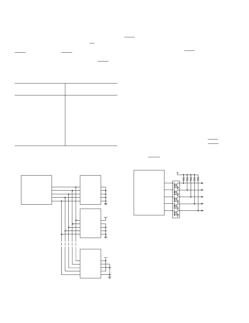
Opto-Isolated Interface
In many process control applications it is necessary to provide
an isolation barrier between the controller and the unit being
controlled. Opto-isolators can provide voltage isolation in ex-
cess of 3 kV. The serial loading structure of the AD7834 makes
it ideal for opto-isolated interfaces as the number of interface
lines is kept to a minimum. Figure 28 shows a 5-channel iso-
lated interface to the AD7834. Multiple devices are connected
to the outputs of the opto-coupler and controlled as explained
above. To reduce the number of opto-isolators, the
PAEN
line
doesn’t need to be controlled if it is not used. If the
PAEN
line
is not controlled by the microcontroller then it should be tied
low at each device. If simultaneous updating of the DACs is not
required, then
LDAC
pin on each part can be tied permanently
low and a further opto-isolator is not needed.
μCONTROLLER
CONTROL OUT
CONTROL OUT
SYNC OUT
SERIAL CLOCK OUT
SERIAL DATA OUT
OPTO-COUPLER
V
CC
TO
PAEN
s
TO
LDAC
s
TO
FSYNC
s
TO SCLKs
TO DINs
Figure 28. Opto-Isolated Interface
Automated Test Equipment
The AD7834/AD7835 is particularly suited for use in an auto-
mated test environment. Figure 29 shows the AD7835 provid-
ing the necessary voltages for the pin driver and the window
comparator in a typical ATE pin electronics configuration. Two
AD588s are used to provide reference voltages for the AD7835.
In the configuration shown, the AD588s are configured so that
the voltage at Pin 1 is 5 V greater than the voltage at Pin 9 and
the voltage at Pin 15 is 5 V less than the voltage at Pin 9.
One of the AD588s is used as a reference for DACs 1 and 2.
These DACs are used to provide high and low levels for the pin
driver. The pin driver may have an associated offset. This can
be nulled by applying an offset voltage to Pin 9 of the AD588.
First, the code 1000 . . . 0000 is loaded into the DAC1 latch
and the pin driver output is set to the DAC1 output. The
相關PDF資料 |
PDF描述 |
|---|---|
| AD7835 | 14-Bit Quad DAC(14位四D/A轉換器) |
| AD7837AR | LC2MOS Complete, Dual 12-Bit MDACs |
| AD7837BN | LC2MOS Complete, Dual 12-Bit MDACs |
| AD7837BQ | 2.7V-5.25V Digital, 5V Analog, 14 Bit, 1.25 MSPS, Serial ADC w/Ref 48-TQFP -40 to 85 |
| AD7837BR | LC2MOS Complete, Dual 12-Bit MDACs |
相關代理商/技術參數 |
參數描述 |
|---|---|
| AD7834AN | 功能描述:IC DAC 14BIT QUAD SRL 28-DIP RoHS:否 類別:集成電路 (IC) >> 數據采集 - 數模轉換器 系列:- 產品培訓模塊:Lead (SnPb) Finish for COTS Obsolescence Mitigation Program 標準包裝:1,000 系列:- 設置時間:1µs 位數:8 數據接口:串行 轉換器數目:8 電壓電源:雙 ± 功率耗散(最大):941mW 工作溫度:0°C ~ 70°C 安裝類型:表面貼裝 封裝/外殼:24-SOIC(0.295",7.50mm 寬) 供應商設備封裝:24-SOIC W 包裝:帶卷 (TR) 輸出數目和類型:8 電壓,單極 采樣率(每秒):* |
| AD7834ANZ | 功能描述:IC DAC 14BIT QUAD SRL 28-DIP RoHS:是 類別:集成電路 (IC) >> 數據采集 - 數模轉換器 系列:- 標準包裝:1 系列:- 設置時間:4.5µs 位數:12 數據接口:串行,SPI? 轉換器數目:1 電壓電源:單電源 功率耗散(最大):- 工作溫度:-40°C ~ 125°C 安裝類型:表面貼裝 封裝/外殼:8-SOIC(0.154",3.90mm 寬) 供應商設備封裝:8-SOICN 包裝:剪切帶 (CT) 輸出數目和類型:1 電壓,單極;1 電壓,雙極 采樣率(每秒):* 其它名稱:MCP4921T-E/SNCTMCP4921T-E/SNRCTMCP4921T-E/SNRCT-ND |
| AD7834AR | 功能描述:IC DAC 14BIT QUAD SRL 28-SOIC RoHS:否 類別:集成電路 (IC) >> 數據采集 - 數模轉換器 系列:- 產品培訓模塊:Lead (SnPb) Finish for COTS Obsolescence Mitigation Program 標準包裝:1,000 系列:- 設置時間:1µs 位數:8 數據接口:串行 轉換器數目:8 電壓電源:雙 ± 功率耗散(最大):941mW 工作溫度:0°C ~ 70°C 安裝類型:表面貼裝 封裝/外殼:24-SOIC(0.295",7.50mm 寬) 供應商設備封裝:24-SOIC W 包裝:帶卷 (TR) 輸出數目和類型:8 電壓,單極 采樣率(每秒):* |
| AD7834AR-REEL | 功能描述:IC DAC 14BIT QUAD SRL 28-SOIC RoHS:否 類別:集成電路 (IC) >> 數據采集 - 數模轉換器 系列:- 標準包裝:2,400 系列:- 設置時間:- 位數:18 數據接口:串行 轉換器數目:3 電壓電源:模擬和數字 功率耗散(最大):- 工作溫度:-40°C ~ 85°C 安裝類型:表面貼裝 封裝/外殼:36-TFBGA 供應商設備封裝:36-TFBGA 包裝:帶卷 (TR) 輸出數目和類型:* 采樣率(每秒):* |
| AD7834ARZ | 功能描述:IC DAC 14BIT QUAD SRL 28-SOIC RoHS:是 類別:集成電路 (IC) >> 數據采集 - 數模轉換器 系列:- 標準包裝:1 系列:- 設置時間:4.5µs 位數:12 數據接口:串行,SPI? 轉換器數目:1 電壓電源:單電源 功率耗散(最大):- 工作溫度:-40°C ~ 125°C 安裝類型:表面貼裝 封裝/外殼:8-SOIC(0.154",3.90mm 寬) 供應商設備封裝:8-SOICN 包裝:剪切帶 (CT) 輸出數目和類型:1 電壓,單極;1 電壓,雙極 采樣率(每秒):* 其它名稱:MCP4921T-E/SNCTMCP4921T-E/SNRCTMCP4921T-E/SNRCT-ND |
發布緊急采購,3分鐘左右您將得到回復。