- 您現在的位置:買賣IC網 > PDF目錄373920 > AD7851ARS (ANALOG DEVICES INC) 14-Bit 333 kSPS Serial A/D Converter PDF資料下載
參數資料
| 型號: | AD7851ARS |
| 廠商: | ANALOG DEVICES INC |
| 元件分類: | ADC |
| 英文描述: | 14-Bit 333 kSPS Serial A/D Converter |
| 中文描述: | 1-CH 14-BIT SUCCESSIVE APPROXIMATION ADC, SERIAL ACCESS, PDSO24 |
| 封裝: | MO-15AG, SSOP-24 |
| 文件頁數: | 22/36頁 |
| 文件大小: | 435K |
| 代理商: | AD7851ARS |
第1頁第2頁第3頁第4頁第5頁第6頁第7頁第8頁第9頁第10頁第11頁第12頁第13頁第14頁第15頁第16頁第17頁第18頁第19頁第20頁第21頁當前第22頁第23頁第24頁第25頁第26頁第27頁第28頁第29頁第30頁第31頁第32頁第33頁第34頁第35頁第36頁
AD7851
–22–
REV. A
System Gain and Offset Interaction
T he inherent architecture of the AD7851 leads to an interaction
between the system offset and gain errors when a system calibra-
tion is performed. T herefore it is recommended to perform the
cycle of a system offset calibration followed by a system gain
calibration twice. Separate system offset and system gain cali-
brations reduce the offset and gain errors to at least the 14-bit
level. By performing a system offset calibration first and a sys-
tem gain calibration second, priority is given to reducing the
gain error to zero before reducing the offset error to zero. If the
system errors are small, a system offset calibration would be per-
formed, followed by a system gain calibration. If the systems er-
rors are large (close to the specified limits of the calibration
range), this cycle would be repeated twice to ensure that the off-
set and gain errors were reduced to at least the 14-bit level. T he
advantage of doing separate system offset and system gain cali-
brations is that the user has more control over when the analog
inputs need to be at the required levels, and the
CONVST
sig-
nal does not have to be used.
Alternatively, a system (gain + offset) calibration can be per-
formed. It is recommended to perform three system (gain + off-
set) calibrations to reduce the offset and gain errors to the 14-bit
level. For the system (gain + offset) calibration priority is given
to reducing the offset error to zero before reducing the gain er-
ror to zero. T hus if the system errors are small then two system
(gain + offset) calibrations will be sufficient. If the system errors
are large (close to the specified limits of the calibration range),
three system (gain + offset) calibrations may be required to re-
duced the offset and gain errors to at least the 14-bit level.
T here will never be any need to perform more than three system
(offset + gain) calibrations.
In Bipolar Mode the midscale error is adjusted for an offset cali-
bration and the positive full-scale error is adjusted for the gain
calibration; in Unipolar Mode the zero-scale error is adjusted
for an offset calibration and the positive full-scale error is ad-
justed for a gain calibration.
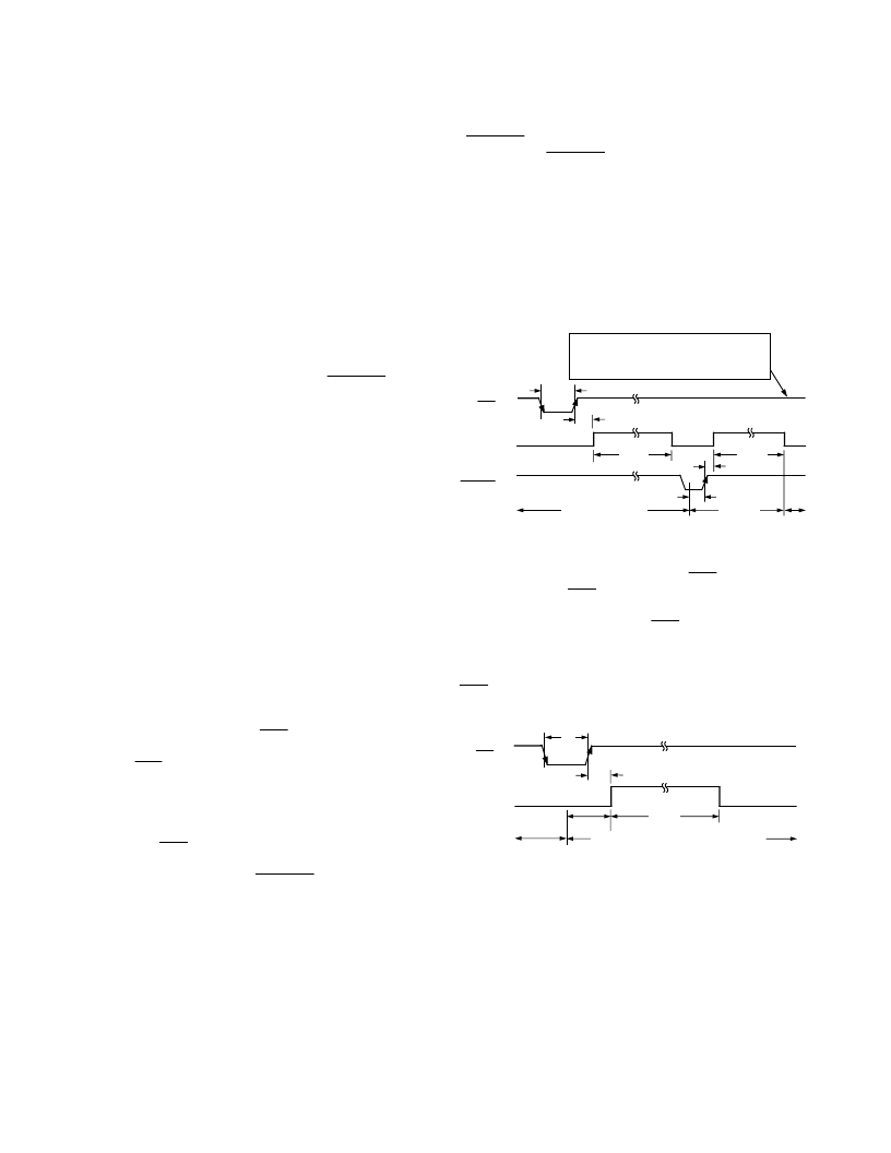
System Calibration T iming
T he calibration timing diagram in Figure 31 is for a full system
calibration where the falling edge of
CAL
initiates an internal
reset before starting a calibration (
note that if the part is in power-
down mode the
CAL
pulse width must take account of the power-up
time)
. If a full system calibration is to be performed in software,
it is easier to perform separate gain and offset calibrations so
that the CONVST bit in the control register does not have to be
programmed in the middle of the system calibration sequence.
T he rising edge of
CAL
starts calibration of the internal DAC
and causes the BUSY line to go high. If the control register is
set for a full system calibration, the
CONVST
must be used
also. T he full-scale system voltage should be applied to the ana-
log input pins from the start of calibration. T he BUSY line will
go low once the DAC and system gain calibration are complete.
Next the system offset voltage is applied to the AIN pin for a
minimum setup time (t
SET UP
) of 100 ns before the rising edge of
the
CONVST
and remain until the BUSY signal goes low. T he
rising edge of the
CONVST
starts the system offset calibration
section of the full system calibration and also causes the BUSY
signal to go high. T he BUSY signal will go low after a time t
CAL2
when the calibration sequence is complete.
T he timing for a system (gain + offset) calibration is very similar
to that of Figure 31, the only difference being that the time
t
CAL1
will be replaced by a shorter time of the order of t
CAL2
as
the internal DAC will not be calibrated. T he BUSY signal will
signify when the gain calibration is finished and when the part is
ready for the offset calibration.
CONVST
(I/P)
AIN (I/P)
t
16
t
SETUP
CAL
(I/P)
BUSY (O/P)
t
1
t
15
t
CAL1
t
CAL2
V
SYSTEM FULL SCALE
V
OFFSET
t
1
= 100ns MIN,
t
14
= 50 MAX,
t
15
= 4
t
CLKIN
MAX,
t
CAL1
= 222228
t
CLKIN
MAX,
t
CAL2
= 27798
t
CLKIN
Figure 31. Timing Diagram for Full System Calibration
T he timing diagram for a system offset or system gain calibra-
tion is shown in Figure 32. Here again the
CAL
is pulsed and
the rising edge of the
CAL
initiates the calibration sequence (or
the calibration can be initiated in software by writing to the con-
trol register). T he rising edge of the
CAL
causes the BUSY line
to go high and it will stay high until the calibration sequence is
finished. T he analog input should be set at the correct level for
a minimum setup time (t
SET UP
) of 100 ns before the rising edge
of
CAL
and stay at the correct level until the BUSY signal goes
low.
AIN (I/P)
t
SETUP
CAL
(I/P)
BUSY (O/P)
t
15
t
CAL2
t
1
V
SYSTEM FULL SCALE
OR V
SYSTEM OFFSET
Figure 32. Timing Diagram for System Gain or System
Offset Calibration
相關PDF資料 |
PDF描述 |
|---|---|
| AD7851KN | 14-Bit 333 kSPS Serial A/D Converter |
| AD7851KR | 14-Bit 333 kSPS Serial A/D Converter |
| AD7853LARS | 3 V to 5 V Single Supply, 200 kSPS 12-Bit Sampling ADCs |
| AD7853L* | Single Supply V.35 Transceiver; Package: SO; No of Pins: 28; Temperature Range: -40°C to +85°C |
| AD7853L | 3 V to 5 V Single Supply, 200 kSPS 12-Bit Sampling ADCs(單電源,200kSPS 12位采樣A/D轉換器) |
相關代理商/技術參數 |
參數描述 |
|---|---|
| AD7851ARS-REEL | 制造商:Analog Devices 功能描述:ADC Single SAR 333ksps 14-bit Serial 24-Pin SSOP T/R |
| AD7851ARSZ | 功能描述:IC ADC 14BIT SRL 333KSPS 24SSOP RoHS:是 類別:集成電路 (IC) >> 數據采集 - 模數轉換器 系列:- 標準包裝:1,000 系列:- 位數:12 采樣率(每秒):300k 數據接口:并聯 轉換器數目:1 功率耗散(最大):75mW 電壓電源:單電源 工作溫度:0°C ~ 70°C 安裝類型:表面貼裝 封裝/外殼:24-SOIC(0.295",7.50mm 寬) 供應商設備封裝:24-SOIC 包裝:帶卷 (TR) 輸入數目和類型:1 個單端,單極;1 個單端,雙極 |
| AD7851ARSZ-REEL | 功能描述:IC ADC 14BIT SRL 333KSPS 24SSOP RoHS:是 類別:集成電路 (IC) >> 數據采集 - 模數轉換器 系列:- 標準包裝:1,000 系列:- 位數:12 采樣率(每秒):300k 數據接口:并聯 轉換器數目:1 功率耗散(最大):75mW 電壓電源:單電源 工作溫度:0°C ~ 70°C 安裝類型:表面貼裝 封裝/外殼:24-SOIC(0.295",7.50mm 寬) 供應商設備封裝:24-SOIC 包裝:帶卷 (TR) 輸入數目和類型:1 個單端,單極;1 個單端,雙極 |
| AD7851ARZ | 功能描述:IC ADC 14BIT SRL 333KSPS 24-SOIC RoHS:是 類別:集成電路 (IC) >> 數據采集 - 模數轉換器 系列:- 標準包裝:1,000 系列:- 位數:12 采樣率(每秒):300k 數據接口:并聯 轉換器數目:1 功率耗散(最大):75mW 電壓電源:單電源 工作溫度:0°C ~ 70°C 安裝類型:表面貼裝 封裝/外殼:24-SOIC(0.295",7.50mm 寬) 供應商設備封裝:24-SOIC 包裝:帶卷 (TR) 輸入數目和類型:1 個單端,單極;1 個單端,雙極 |
| AD7851ARZ3 | 制造商:AD 制造商全稱:Analog Devices 功能描述:14-Bit 333 kSPS Serial A/D Converter |
發布緊急采購,3分鐘左右您將得到回復。