- 您現在的位置:買賣IC網 > PDF目錄373920 > AD7858LAR (ANALOG DEVICES INC) 3 V to 5 V Single Supply, 200 kSPS 8-Channel, 12-Bit Sampling ADC PDF資料下載
參數資料
| 型號: | AD7858LAR |
| 廠商: | ANALOG DEVICES INC |
| 元件分類: | ADC |
| 英文描述: | 3 V to 5 V Single Supply, 200 kSPS 8-Channel, 12-Bit Sampling ADC |
| 中文描述: | 8-CH 12-BIT SUCCESSIVE APPROXIMATION ADC, SERIAL ACCESS, PDSO24 |
| 封裝: | SOIC-24 |
| 文件頁數: | 17/32頁 |
| 文件大小: | 315K |
| 代理商: | AD7858LAR |
第1頁第2頁第3頁第4頁第5頁第6頁第7頁第8頁第9頁第10頁第11頁第12頁第13頁第14頁第15頁第16頁當前第17頁第18頁第19頁第20頁第21頁第22頁第23頁第24頁第25頁第26頁第27頁第28頁第29頁第30頁第31頁第32頁
AD7858/AD7858L
REV. B
–17–
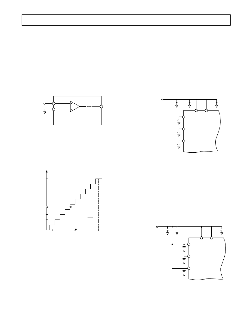
Input Range
The analog input range for the AD7858/AD7858L is 0 V to
V
REF
. The AIN(
–
) pin on the AD7858/AD7858L can be biased
up above AGND, if required. The advantage of biasing the
lower end of the analog input range away from AGND is that
the user does not need to have the analog input swing all the
way down to AGND. This has the advantage in true single-
supply applications that the input amplifier does not need to
swing all the way down to AGND. The upper end of the analog
input range is shifted up by the same amount. Care must be
taken so that the bias applied does not shift the upper end of the
analog input above the AV
DD
supply. In the case where the
reference is the supply, AV
DD
, the AIN(
–
) must be tied to
AGND.
AD7858/
AD7858L
AIN(+)
AIN(
–
)
TRACK AND HOLD
AMPLIFIER
DOUT
STRAIGHT
BINARY
FORMAT
V
IN
= 0 TO V
REF
Figure 14. 0 to V
REF
Input Configuration
Transfer Function
For the AD7858/AD7858L input range the designed code tran-
sitions occur midway between successive integer LSB values
(i.e., 1/2 LSB, 3/2 LSBs, 5/2 LSBs . . . FS
–
3/2 LSBs). The
output coding is straight binary with 1 LSB = FS/4096 = 3.3 V/
4096 = 0.8 mV when V
REF
= 3.3 V. The ideal input/output
transfer characteristic is shown in Figure 15.
OUTPUT
CODE
111...111
111...110
111...101
111...100
000...011
000...010
000...001
000...000
1LSB =4096
0V 1LSB
+FS
–
1LSB
V
IN
= (AIN(+)
–
AIN(
–
)), INPUT VOLTAGE
Figure 15. AD7858/AD7858L Transfer Characteristic
REFERENCE SECTION
For specified performance, it is recommended that when using
an external reference this reference should be between 2.3 V
and the analog supply AV
DD
. The connections for the relevant
reference pins are shown in the typical connection diagrams. If
the internal reference is being used, the REF
IN
/REF
OUT
pin
should have a 100 nF capacitor connected to AGND very close
to the REF
IN
/REF
OUT
pin. These connections are shown in
Figure 16.
If the internal reference is required for use external to the ADC,
it should be buffered at the REF
IN
/REF
OUT
pin and a 100 nF
connected from this pin to AGND. The typical noise performance
for the internal reference, with 5 V supplies, is 150 nV/
√
Hz
@
1 kHz and dc noise is 100
μ
V p-p.
0.1 F
0.01 F
0.1 F
0.1 F
10 F
0.1 F
AD7858/
AD7858L
ANALOG SUPPLY
+3V TO +5V
AV
DD
DV
DD
C
REF1
C
REF2
REF
IN
/REF
OUT
Figure 16. Relevant Connections When Using Internal
Reference
The other option is that the REF
IN
/REF
OUT
pin be overdriven
by connecting it to an external reference. This is possible due to
the series resistance from the REF
IN
/REF
OUT
pin to the internal
reference. This external reference can have a range that includes
AV
DD
. When using AV
DD
as the reference source, the 100 nF
capacitor from the REF
IN
/REF
OUT
pin to AGND should be as
close as possible to the REF
IN
/REF
OUT
pin, and also the C
REF1
pin should be connected to AV
DD
to keep this pin at the same
level as the reference. The connections for this arrangement are
shown in Figure 17. When using AV
DD
it may be necessary to
add a resistor in series with the AV
DD
supply. This will have the
effect of filtering the noise associated with the AV
DD
supply.
0.1 F
0.01 F
0.1 F
0.1 F
10 F
0.1 F
AD7858/
AD7858L
ANALOG SUPPLY
+3V TO +5V
AV
DD
DV
DD
C
REF1
C
REF2
REF
IN
/REF
OUT
Figure 17. Relevant Connections When Using AV
DD
as the
Reference
相關PDF資料 |
PDF描述 |
|---|---|
| AD7858LBN | 3 V to 5 V Single Supply, 200 kSPS 8-Channel, 12-Bit Sampling ADC |
| AD7858LBR | 3 V to 5 V Single Supply, 200 kSPS 8-Channel, 12-Bit Sampling ADC |
| AD7858L* | 3 V to 5 V Single Supply. 200 kSPS 8-Channel. 12-Bit Sampling ADC |
| AD7862AR-2 | Simultaneous Sampling Dual 250 kSPS 12-Bit ADC |
| AD7862SQ-10 | Simultaneous Sampling Dual 250 kSPS 12-Bit ADC |
相關代理商/技術參數 |
參數描述 |
|---|---|
| AD7858LAR3 | 制造商:AD 制造商全稱:Analog Devices 功能描述:3 V to 5 V Single Supply, 200 kSPS 8-Channel, 12-Bit Sampling ADC |
| AD7858LAR-REEL | 制造商:Analog Devices 功能描述:ADC Single SAR 100ksps 12-bit Serial 24-Pin SOIC W T/R |
| AD7858LARS | 功能描述:IC ADC 12BIT 8CH SRL 24-SSOP RoHS:否 類別:集成電路 (IC) >> 數據采集 - 模數轉換器 系列:- 標準包裝:1,000 系列:- 位數:12 采樣率(每秒):300k 數據接口:并聯 轉換器數目:1 功率耗散(最大):75mW 電壓電源:單電源 工作溫度:0°C ~ 70°C 安裝類型:表面貼裝 封裝/外殼:24-SOIC(0.295",7.50mm 寬) 供應商設備封裝:24-SOIC 包裝:帶卷 (TR) 輸入數目和類型:1 個單端,單極;1 個單端,雙極 |
| AD7858LARS3 | 制造商:AD 制造商全稱:Analog Devices 功能描述:3 V to 5 V Single Supply, 200 kSPS 8-Channel, 12-Bit Sampling ADC |
| AD7858LARS-REEL | 功能描述:IC ADC 12BIT 8CH SRL 24-SSOP RoHS:否 類別:集成電路 (IC) >> 數據采集 - 模數轉換器 系列:- 標準包裝:1,000 系列:- 位數:12 采樣率(每秒):300k 數據接口:并聯 轉換器數目:1 功率耗散(最大):75mW 電壓電源:單電源 工作溫度:0°C ~ 70°C 安裝類型:表面貼裝 封裝/外殼:24-SOIC(0.295",7.50mm 寬) 供應商設備封裝:24-SOIC 包裝:帶卷 (TR) 輸入數目和類型:1 個單端,單極;1 個單端,雙極 |
發布緊急采購,3分鐘左右您將得到回復。