- 您現在的位置:買賣IC網 > PDF目錄373921 > AD7864AS-2 (ANALOG DEVICES INC) 4-Channel, Simultaneous Sampling, High Speed, 12-Bit ADC PDF資料下載
參數資料
| 型號: | AD7864AS-2 |
| 廠商: | ANALOG DEVICES INC |
| 元件分類: | ADC |
| 英文描述: | 4-Channel, Simultaneous Sampling, High Speed, 12-Bit ADC |
| 中文描述: | 4-CH 12-BIT SUCCESSIVE APPROXIMATION ADC, PARALLEL ACCESS, PQFP44 |
| 封裝: | PLASTIC, MO-112-AA, MQFP-44 |
| 文件頁數: | 10/19頁 |
| 文件大小: | 214K |
| 代理商: | AD7864AS-2 |
AD7864
–10–
REV. A
AD7864-3
Figure 4 shows the analog input section of the AD7864-3. The
analog input range is
±
2.5 V on the V
IN1A
input. The V
IN1B
input can be left unconnected but if it is connected to a poten-
tial then that potential must be AGND.
2.5V
REFERENCE
T/H
TO ADC
REFERENCE
CIRCUITRY
6k
V
R2
TO INTERNAL
COMPARATOR
AD7864-3
R1
V
IN1B
V
IN1A
V
REF
Figure 4. AD7864-3 Analog Input Structure
For the AD7864-3, R1 = 6 k
and R2 = 6 k
.
As a result, the
V
IN1A
input should be driven from a low impedance source. The
resistor input stage is followed by the high input impedance
stage of the track/hold amplifier.
The designed code transitions take place midway between
successive integer LSB values (i.e., 1/2 LSB, 3/2 LSBs, 5/2 LSBs,
etc.) LSB size is given by the formula, 1 LSB = FSR/4096.
Output coding is 2s complement binary with 1 LSB = FSR/
4096 = 5 V/4096 = 1.22 mV. The ideal input/output transfer
function for the AD7864-3 is shown in Table III.
Table III. Ideal Input/Output Code Table for the AD7864-3
Analog Input
l
+FSR/2 – 3/2 LSB
2
+FSR/2 – 5/2 LSB
+FSR/2 – 7/2 LSB
Digital Output Code Transition
011 . . . 110 to 011 . . . 111
011 . . . 101 to 011 . . . 110
011 . . . 100 to 011 . . . 101
AGND + 3/2 LSB
AGND + 1/2 LSB
AGND – 1/2 LSB
AGND – 3/2 LSB
000 . . . 001 to 000 . . . 010
000 . . . 000 to 000 . . . 001
111 . . . 111 to 000 . . . 000
111 . . . 110 to 111 . . . 111
–FSR/2 + 5/2 LSB
–FSR/2 + 3/2 LSB
–FSR/2 + 1/2 LSB
100 . . . 010 to 100 . . . 011
100 . . . 001 to 100 . . . 010
100 . . . 000 to 100 . . . 001
NOTES
1
FSR is full-scale range is 5 V, with V
= +2.5 V.
2
1 LSB = FSR/4096 = 1.22 mV (
±
2.5 V - AD7864-3) with V
REF
= +2.5 V.
SELECTING A CONVERSION SEQUENCE
Any subset of the four channels VIN1 to VIN4 can be selected
for conversion. The selected channels are converted in an
ascending order. For example if the channel selection includes
VIN4, VIN1 and VIN3 then the conversion sequence will be
VIN1, VIN3 and then VIN4. The conversion sequence selection
my be made by using either the hardware channel select input
pins (SL1 through SL4) or programming the channel select
register. A logic high on a hardware channel select pin (or logic
one in the channel select register) when
CONVST
goes logic
high, marks the associated analog input channel for inclusion in
the conversion sequence.
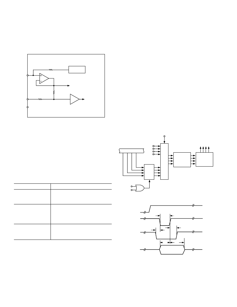
Figure 5 shows the arrangement used. The
H
/S SEL controls a
multiplexer which selects the source of the conversion sequence
information, i.e., from the Hardware channel select pins (SL1 to
SL4) or from the channel selection register. When a conversion
is started the output from the multiplexer is latched until the
end of the conversion sequence. The data bus Bits DB0 to DB3
(DB0 representing Channel 1 through DB3 representing Chan-
nel 4) are bidirectional and become inputs to the channel select
register when
RD
is logic high and
CS
and
WR
are logic low.
The logic state on DB0 to DB3 is latched into the channel select
register when
WR
goes logic high.
M
U
L
T
I
P
L
E
X
E
R
DATA BUS
D1
D2
D0
D3
WR
CS
WR
CHANNEL SELECT
REGISTER
SL1
SL2
SL3
SL4
HARDWARE CHANNEL
SELECT PINS
H
/S
LATCH
SEQUENCER
TRANSPARENT WHILE WAITING FOR
CONVST
. LATCHED ON THE RISING
EDGE OF
CONVST
AND DURING A
CONVERSION SEQUENCE.
SELECT INDIVIDUAL
TRACK-AND-HOLDS
FOR CONVERSION
Figure 5. Channel Select Inputs and Registers
RD
WR
CS
DATA
t
16
t
17
t
14
t
15
t
13
DATA IN
Figure 6. Channel Selection via Software Control
相關PDF資料 |
PDF描述 |
|---|---|
| AD7864AS-3 | 4-Channel, Simultaneous Sampling, High Speed, 12-Bit ADC |
| AD7864AS | IC-SM-12-BIT ADC |
| AD7865YS-1 | Four-Channel, Simultaneous Sampling, Fast, 14-Bit ADC |
| AD7865YS-2 | Four-Channel, Simultaneous Sampling, Fast, 14-Bit ADC |
| AD7865YS-3 | Four-Channel, Simultaneous Sampling, Fast, 14-Bit ADC |
相關代理商/技術參數 |
參數描述 |
|---|---|
| AD7864AS-2REEL | 制造商:Analog Devices 功能描述:ADC Single SAR 520ksps 12-bit Parallel 44-Pin MQFP T/R |
| AD7864AS-2Z | 制造商:Analog Devices 功能描述:ADC 12BIT 4CH 500KSPS 44MQ 制造商:Analog Devices 功能描述:ADC, 12BIT, 4CH, 500KSPS, 44MQFP; Resolution (Bits):12bit; Sampling Rate:520kSPS; Supply Voltage Type:Single; Supply Voltage Min:4.75V; Supply Voltage Max:5.25V; Supply Current:24mA; Digital IC Case Style:MQFP; No. of Pins:44; Input ;RoHS Compliant: Yes |
| AD7864AS-3 | 制造商:Analog Devices 功能描述:ADC Single SAR 520ksps 12-bit Parallel 44-Pin MQFP 制造商:Analog Devices 功能描述:IC 12-BIT ADC |
| AD7864AS-3REEL | 制造商:Analog Devices 功能描述:ADC Single SAR 520ksps 12-bit Parallel 44-Pin MQFP T/R |
| AD7864AS-3Z | 制造商:Analog Devices 功能描述:ADC 12BIT 4CH 500KSPS 44MQ 制造商:Analog Devices 功能描述:ADC, 12BIT, 4CH, 500KSPS, 44MQFP; Resolution (Bits):12bit; Sampling Rate:520kSPS; Supply Voltage Type:Single; Supply Voltage Min:4.75V; Supply Voltage Max:5.25V; Supply Current:24mA; Digital IC Case Style:MQFP; No. of Pins:44; Input ;RoHS Compliant: Yes |
發布緊急采購,3分鐘左右您將得到回復。