- 您現(xiàn)在的位置:買賣IC網(wǎng) > PDF目錄373921 > AD7864AS-2 (ANALOG DEVICES INC) 4-Channel, Simultaneous Sampling, High Speed, 12-Bit ADC PDF資料下載
參數(shù)資料
| 型號: | AD7864AS-2 |
| 廠商: | ANALOG DEVICES INC |
| 元件分類: | ADC |
| 英文描述: | 4-Channel, Simultaneous Sampling, High Speed, 12-Bit ADC |
| 中文描述: | 4-CH 12-BIT SUCCESSIVE APPROXIMATION ADC, PARALLEL ACCESS, PQFP44 |
| 封裝: | PLASTIC, MO-112-AA, MQFP-44 |
| 文件頁數(shù): | 12/19頁 |
| 文件大小: | 214K |
| 代理商: | AD7864AS-2 |
AD7864
–12–
REV. A
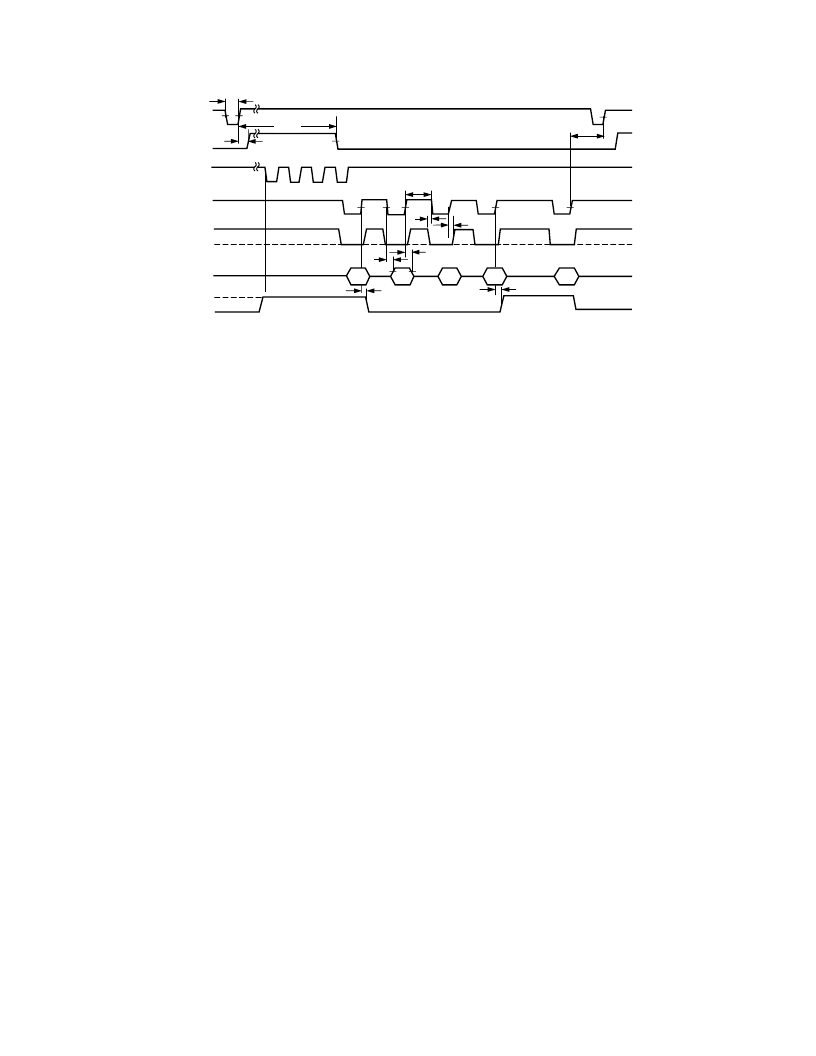
Reading After the Conversion Sequence
Figure 8 shows the same conversion sequence as Figure 7. In
this case, however, the results of the four conversions (on VIN1
to VIN4) are read after all conversions have finished, i.e., when
BUSY goes logic low. The FRSTDATA signal goes logic high
at the end of the first conversion just prior to
EOC
going logic
low. As mentioned previously FRSTDATA has an indetermi-
nate state after initial power up, therefore FRSTDATA may
already be logic high. Unlike the case when reading between
each conversion the output data register pointer is incremented
on the rising edge of
RD
because the next conversion result is
available. This means FRSTDATA will go logic low after the
first rising edge on
RD
.
Successive read operations will access the remaining conversion
results in an ascending channel order. Each read operation
increments the output data register pointer. The read operation
that accesses the last conversion result causes the output data
register pointer to be reset so that the next read operation will
access the first conversion result again. This is shown in Figure
8 with the fifth read after BUSY goes low accessing the result of
the conversion on VIN1. Thus the output data registers act as a
circular buffer in which the conversion results may be continu-
ally accessed. The FRSTDATA signal will go high when the
first conversion result is available.
Data is enabled onto the data bus DB0 to DB11 using
CS
and
RD
. Both
CS
and
RD
have the same functionality as described
in the previous section. There are no restrictions or perfor-
mance implications associated to the position of the read opera-
tions after BUSY goes low. The only restriction is that there is
minimum time between read operations. Notice also that a
“Quiet Time” is needed before the start of the next conversion.
Using an External Clock
The logic input
INT
/EXT CLK allows the user to operate the
AD7864 using the internal clock oscillator or an external clock.
The optimum performance is achieved by using the internal
clock on the AD7864. The highest external clock frequency
allowed is 5 MHz. This means a conversion time of 2.6
μ
s
compared to 1.65
μ
s using the internal clock. In some instances,
however, it may be useful to use an external clock when high
throughput rates are not required. For example, two or more
AD7864s may be synchronized by using the same external clock
for all devices. In this way there is no latency between output
logic signals like
EOC
due to differences in the frequency of the
internal clock oscillators. Figure 9 shows how the various logic
outputs are synchronized to the CLK signal. Each conversion
requires 14 clocks. The output data register pointer is reset to
point to the first register location on the falling edge of the 12
clock cycle of the first conversion in the conversion sequence—
See Accessing the Output Data Registers. At this point the logic
output FRSTDATA goes logic high. The result of the first
conversion is transferred to the output data registers on the
falling edge of the 13 clock cycle. The FRSTDATA signal is
reset on the falling edge of the 13 clock cycle of the next
conversion, i.e., when the result of the second conversion is
transferred to its output data register. As mentioned previously,
the pointer is incremented by the rising edge of the
RD
signal if
the result of the next conversion is available. The
EOC
signal
goes logic low on the falling edge of the 13 clock cycle and is
reset high again on the falling edge of the 14 clock cycle.
t
10
t
8
t
4
t
3
t
6
t
1
QUIET
TIME
DATA
CONVST
BUSY
EOC
FRSTDATA
RD
CS
V
IN1
V
IN2
V
IN3
V
IN4
V
IN1
t
BUSY
t
2
t
10
t
7
Figure 8. Timing Diagram, Reading After the Conversion Sequence
相關(guān)PDF資料 |
PDF描述 |
|---|---|
| AD7864AS-3 | 4-Channel, Simultaneous Sampling, High Speed, 12-Bit ADC |
| AD7864AS | IC-SM-12-BIT ADC |
| AD7865YS-1 | Four-Channel, Simultaneous Sampling, Fast, 14-Bit ADC |
| AD7865YS-2 | Four-Channel, Simultaneous Sampling, Fast, 14-Bit ADC |
| AD7865YS-3 | Four-Channel, Simultaneous Sampling, Fast, 14-Bit ADC |
相關(guān)代理商/技術(shù)參數(shù) |
參數(shù)描述 |
|---|---|
| AD7864AS-2REEL | 制造商:Analog Devices 功能描述:ADC Single SAR 520ksps 12-bit Parallel 44-Pin MQFP T/R |
| AD7864AS-2Z | 制造商:Analog Devices 功能描述:ADC 12BIT 4CH 500KSPS 44MQ 制造商:Analog Devices 功能描述:ADC, 12BIT, 4CH, 500KSPS, 44MQFP; Resolution (Bits):12bit; Sampling Rate:520kSPS; Supply Voltage Type:Single; Supply Voltage Min:4.75V; Supply Voltage Max:5.25V; Supply Current:24mA; Digital IC Case Style:MQFP; No. of Pins:44; Input ;RoHS Compliant: Yes |
| AD7864AS-3 | 制造商:Analog Devices 功能描述:ADC Single SAR 520ksps 12-bit Parallel 44-Pin MQFP 制造商:Analog Devices 功能描述:IC 12-BIT ADC |
| AD7864AS-3REEL | 制造商:Analog Devices 功能描述:ADC Single SAR 520ksps 12-bit Parallel 44-Pin MQFP T/R |
| AD7864AS-3Z | 制造商:Analog Devices 功能描述:ADC 12BIT 4CH 500KSPS 44MQ 制造商:Analog Devices 功能描述:ADC, 12BIT, 4CH, 500KSPS, 44MQFP; Resolution (Bits):12bit; Sampling Rate:520kSPS; Supply Voltage Type:Single; Supply Voltage Min:4.75V; Supply Voltage Max:5.25V; Supply Current:24mA; Digital IC Case Style:MQFP; No. of Pins:44; Input ;RoHS Compliant: Yes |
發(fā)布緊急采購,3分鐘左右您將得到回復(fù)。